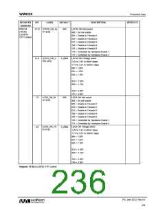
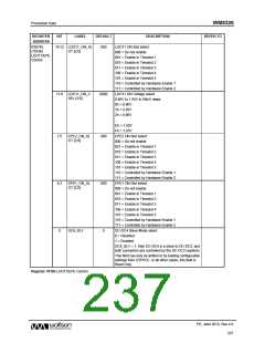
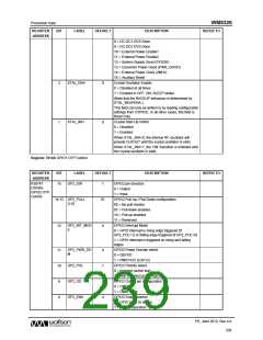
WM8326
Production Data
REFER TO
REGISTER
ADDRESS
BIT
LABEL
DEFAULT
DESCRIPTION
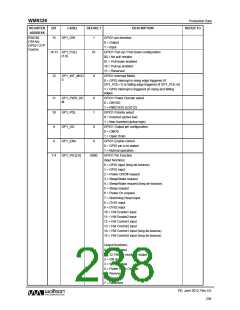
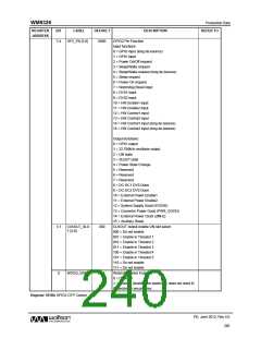
GP2_FN [3:0]
GPIO2 Pin Function
Input functions:
7:4
0000
0 = GPIO input (long de-bounce)
1 = GPIO input
2 = Power On/Off request
3 = Sleep/Wake request
4 = Sleep/Wake request (long de-bounce)
5 = Sleep request
6 = Power On request
7 = Watchdog Reset input
8 = DVS1 input
9 = DVS2 input
10 = HW Enable1 input
11 = HW Enable2 input
12 = HW Control1 input
13 = HW Control2 input
14 = HW Control1 input (long de-bounce)
15 = HW Control2 input (long de-bounce)
Output functions:
0 = GPIO output
1 = 32.768kHz oscillator output
2 = ON state
3 = SLEEP state
4 = Power State Change
5 = Reserved
6 = Reserved
7 = Reserved
8 = DC-DC1 DVS Done
9 = DC-DC2 DVS Done
10 = External Power Enable1
11 = External Power Enable2
12 = System Supply Good (SYSOK)
13 = Converter Power Good (PWR_GOOD)
14 = External Power Clock (2MHz)
15 = Auxiliary Reset
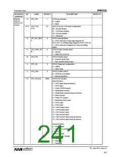
CLKOUT_SLO
T [2:0]
CLKOUT output enable ON slot select
000 = Do not enable
3:1
000
001 = Enable in Timeslot 1
010 = Enable in Timeslot 2
011 = Enable in Timeslot 3
100 = Enable in Timeslot 4
101 = Enable in Timeslot 5
110 = Do not enable
111 = Do not enable
WDOG_ENA
Watchdog Timer Enable
0 = Disabled
0
1
1 = Enabled (enables the watchdog; does not reset it)
Protected by security key.
Register 781Bh GPIO2 OTP Control
PD, June 2012, Rev 4.0
240
w

 WOLFSON [ WOLFSON MICROELECTRONICS PLC ]