WM8321
Production Data
REGISTER
ADDRESS
BIT
LABEL
DEFAULT
DESCRIPTION
REFER TO
R30727
(7807h)
Unique ID 8
UNIQUE_ID
[15:0]
Unique ID, Word 0
15:0
0000_0000
_0000_000
0
Register 7807h Unique ID 8
REGISTER
ADDRESS
BIT
LABEL
DEFAULT
DESCRIPTION
REFER TO
R30736
(7810h)
Customer
OTP ID
OTP_AUTO_P
ROG
If this bit is set when bootstrap data is loaded from ICE
(in development mode), then the ICE contents will be
programmed in the OTP.
15
0
OTP_CUST_ID
[13:0]
This field is checked when an ‘ON’ transition is
requested. A non-zero value is used to confirm valid
data.
14:1
0
00_0000_0
000_0000
OTP_CUST_FI
NAL
If OTP_CUST_FINAL is set in the OTP and also set in
the DCRW, then no further Writes are possible to the
OTP.
0
Register 7810h Customer OTP ID
REGISTER
ADDRESS
BIT
LABEL
DEFAULT
DESCRIPTION
REFER TO
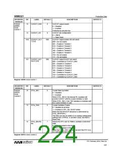
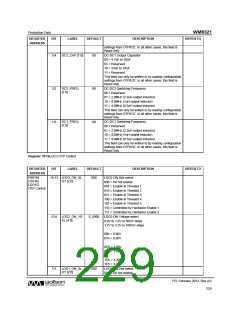
R30737
(7811h) DC1
OTP Control
DC2_ON_SLO
T [2:0]
DC-DC2 ON Slot select
15:13
000
000 = Do not enable
001 = Enable in Timeslot 1
010 = Enable in Timeslot 2
011 = Enable in Timeslot 3
100 = Enable in Timeslot 4
101 = Enable in Timeslot 5
110 = Controlled by Hardware Enable 1
111 = Controlled by Hardware Enable 2
DC-DC2 ON Voltage select
DC2_ON_VSE
L [6:2]
12:8
0_0000
DC2_ON_VSEL [6:0] selects the DC-DC2 output
voltage from 0.6V to 1.8V in 12.5mV steps.
DC2_ON_VSEL [6:2] controls the voltage in 50mV
steps.
DC2_ON_VSEL [6:0] is coded as follows:
00h to 08h = 0.6V
09h = 0.6125V
…
48h = 1.4V (see note)
…
67h = 1.7875V
68h to 7Fh = 1.8V
Note - Maximum output voltage selection in 4MHz
switching mode is 48h (1.4V).
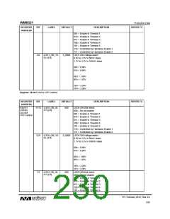
DC1_ON_SLO
T [2:0]
DC-DC1 ON Slot select
000 = Do not enable
7:5
000
001 = Enable in Timeslot 1
010 = Enable in Timeslot 2
011 = Enable in Timeslot 3
PD, February 2012, Rev 4.0
226
w

 WOLFSON [ WOLFSON MICROELECTRONICS PLC ]