WM8321
Production Data
REFER TO
REGISTER
ADDRESS
BIT
LABEL
DEFAULT
DESCRIPTION
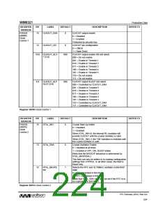
110 = Controlled by Hardware Enable 1
111 = Controlled by Hardware Enable 2
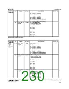
DC-DC3 ON Voltage select
DC3_ON_VSE
L [6:2]
4:0
0_0000
DC3_ON_VSEL [6:0] selects the DC-DC3 output
voltage from 0.85V to 3.4V in 25mV steps.
DC3_ON_VSEL [6:2] controls the voltage in 100mV
steps.
DC3_ON_VSEL [6:0] is coded as follows:
00h = 0.85V
01h = 0.875V
…
65h = 3.375V
66h to 7Fh = 3.4V
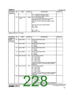
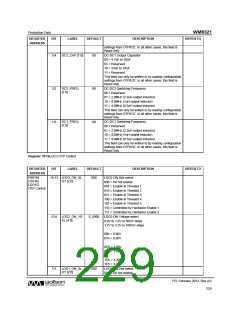
Register 7812h DC2 OTP Control
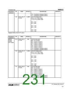
REGISTER
ADDRESS
BIT
LABEL
DEFAULT
DESCRIPTION
REFER TO
R30739
(7813h) DC3
OTP Control
DC4_PHASE
DC-DC4 Clock Phase Control
0 = Normal
15
0
1 = Inverted
DC3_PHASE
DC2_PHASE
DC1_PHASE
DC-DC3 Clock Phase Control
0 = Normal
14
13
12
0
1
1 = Inverted
DC-DC2 Clock Phase Control
0 = Normal
1 = Inverted
DC-DC1 Clock Phase Control
0 = Normal
0
1 = Inverted
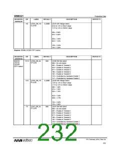
11:10 DC4_CAP [1:0]
00
DC-DC4 Output Capacitor
00 = 10uF to 20uF
01 = 10uF to 20uF
10 = 22uF to 45uF
11 = 47uF to 100uF
This field can only be written to by loading configuration
settings from OTP/ICE. In all other cases, this field is
Read Only.
DC3_CAP [1:0]
DC-DC3 Output Capacitor
00 = 10uF to 20uF
01 = 10uF to 20uF
10 = 22uF to 45uF
11 = 47uF to 100uF
9:8
00
This field can only be written to by loading configuration
settings from OTP/ICE. In all other cases, this field is
Read Only.
DC2_CAP [1:0]
DC-DC2 Output Capacitor
00 = 4.7uF to 20uF
7:6
00
01 = Reserved
10 = 22uF to 47uF
11 = Reserved
This field can only be written to by loading configuration
PD, February 2012, Rev 4.0
228
w

 WOLFSON [ WOLFSON MICROELECTRONICS PLC ]