W90N745CD/W90N745CDG
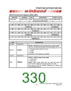
31
23
15
7
30
22
14
6
29
21
13
5
28
20
12
4
27
RESERVED
19
26
18
10
2
25
17
9
24
16
8
RESERVED
11
RESERVED
3
1
0
RESERVED
DATAIN1[1:0]
BITS
DESCRIPTION
[31:2]
RESERVED
-
Port1 input data register
[1:0]
DATAIN1
The DATAIN1 indicates the status of each GPIO19~GPIO18 pin
regardless of its operation mode. The reserved bits are read as 0s.
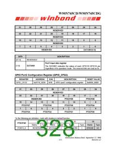
GPIO Port2 Configuration Register (GPIO_CFG2)
REGISTER
ADDRESS
R/W
DESCRIPTION
RESET VALUE
GPIO_CFG2
0xFFF8_3020
R/W
GPIO port2 configuration register
0x0000_0000
31
23
30
22
29
21
28
27
19
11
3
26
18
10
2
25
17
9
24
RESERVED
20
12
4
16
PT2CFG8
8
RESERVED
PT2CFG9
PT2CFG5
PT2CFG1
15
14
13
5
PT2CFG7
7
PT2CFG6
PT2CFG2
PT2CFG4
0
6
1
PT2CFG3
PT2CFG0
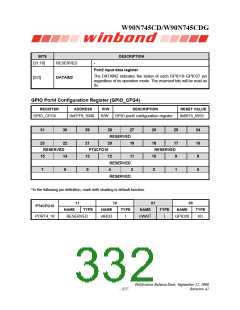
*In the following pin definition, mark with shading is default function.
11
Name
RESERVED
10
Name
KPCOL0
01
Name
PHY_RXERR
00
PT2CFG0
Type
Type
I
Type
Name
Type
I/O
PORT2_0
I
GPIO20
Publication Release Date: September 22, 2006
Revision A2
- 323 -

 WINBOND [ WINBOND ]