W90N745CD/W90N745CDG
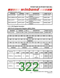
BITS
DESCRIPTION
[31:20]
RESERVED
-
GPIO3 -GPIO0 port pin internal pull-up resister enable
There are 4 bits for this register, the corresponding bit is set to “1”
will enable pull-up resister on IO pin.
1 = enable
0 = disable
[19:16]
PUPEN0
After power on the pull-up resisters are disabled.
NOTE: GPIO4 is used as AC97 BITCLK input, an IO pad with
Schmitt trigger input buffer PDB04SDGZ is implemented for this
pin. Due to TSMC IO library without pull-up register, an external
pull-up resister is necessary.
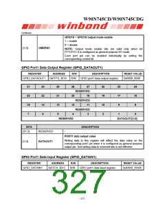
[15:5]
[4:0]
RESERVED
GPIO4 ~GPIO0 output mode enable
1 = output mode
0 = input mode
OMDEN0
NOTE: Output mode enable bits are valid only when bit
PT0CFG4-0 is configured as general purpose I/O mode.
Each port pin can be enabled individually by setting the
corresponding control bit.
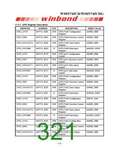
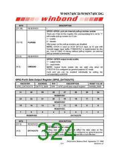
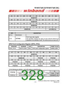
GPIO Port0 Data Output Register (GPIO_DATAOUT0)
REGISTER
ADDRESS
R/W
DESCRIPTION
RESET VALUE
GPIO_DATAOUT0
0xFFF8_3008
R/W
GPIO port0 data output register
0x0000_0000
31
23
15
7
30
22
14
6
29
21
13
5
28
27
26
18
10
25
17
9
24
16
8
RESERVED
20
12
19
RESERVED
11
RESERVED
4
3
2
1
0
RESERVED
DATAOUT0
BITS
DESCRIPTION
[31:5]
RESERVED
-
PORT0 data output value
Writing data to this register will reflect the data value on the
corresponding port0 pin when it is configured as general purpose
output pin. And writing data to reserved bits is not effective.
[4:0]
DATAOUT0
Publication Release Date: September 22, 2006
- 319 -
Revision A2

 WINBOND [ WINBOND ]