W90N745CD/W90N745CDG
y
y
y
y
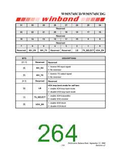
Line break generation and detection
False start bit detection
Full prioritized interrupt system controls
Loop back mode for internal diagnostic testing
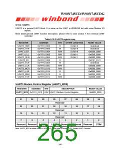
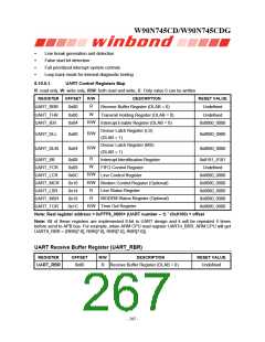
6.10.5.1.
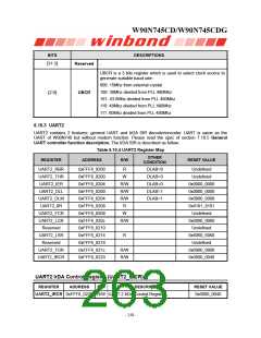
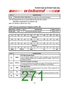
UART Control Registers Map
R: read only, W: write only, R/W: both read and write, C: Only value 0 can be written
REGISTER OFFSET R/W
DESCRIPTION
RESET VALUE
Undefined
R
W
UART_RBR
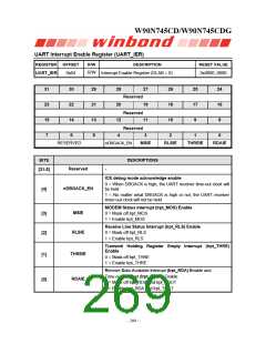
UART_THR
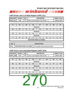
UART_IER
0x00
0x00
0x04
Receive Buffer Register (DLAB = 0)
Transmit Holding Register (DLAB = 0)
Undefined
R/W
Interrupt Enable Register (DLAB = 0)
Divisor Latch Register (LS)
(DLAB = 1)
0x0000_0000
R/W
R/W
UART_DLL
UART_DLM
0x00
0x04
0x0000_0000
0x0000_0000
Divisor Latch Register (MS)
(DLAB = 1)
R
W
UART_IIR
0x08
0x08
0x0C
0x10
0x14
0x18
0x1C
Interrupt Identification Register
0x8181_8181
Undefined
UART_FCR
UART_LCR
UART_MCR
UART_LSR
UART_MSR
UART_TOR
FIFO Control Register
R/W
R/W
R
Line Control Register
0x0000_0000
0x0000_0000
0x6060_6060
0x0000_0000
0x0000_0000
Modem Control Register (Optional)
Line Status Register
R
MODEM Status Register (Optional)
R/W Time Out Register
Note: Real register address = 0xFFF8_0000+ (UART number – 1) * (0x0100) + offset
Note: All of these registers are implemented 8-bit in UART design and it will be repeated 4 times
before send to APB bus. For example, when ARM CPU read register UARTn_BRR, ARM CPU will get
UART0_RBR = {RBR[7:0], RBR[7:0], RBR[7:0], RBR[7:0]}.
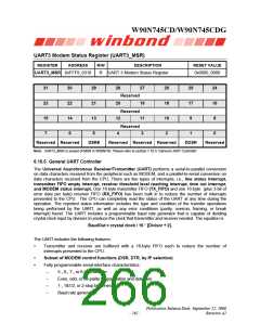
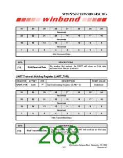
UART Receive Buffer Register (UART_RBR)
REGISTER
OFFSET
R/W
DESCRIPTION
RESET VALUE
0x00
R
Receive Buffer Register (DLAB = 0)
Undefined
UART_RBR
- 262 -

 WINBOND [ WINBOND ]