W83759A
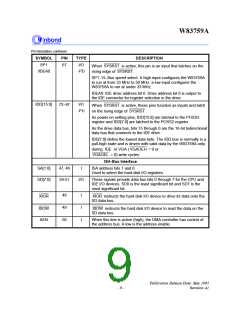
PIN DESCRIPTION
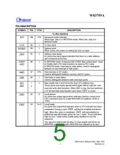
SYMBOL
PIN
TYPE
DESCRIPTION
VL-Bus Interface
Advanced mode indicator.
ADV
100
I-PU
When high, chip is in W83759A mode. When low, chip is in
W83759 mode.
LCLK
89
99
I
I
VL-Bus clock.
System reset.
SYSRST
When active, the power-on setting pin acts as input.
95
98
I
I
Address data strobe.
An active low input signal indicates that there is a valid address
and command on the bus.
LADS
IORDY
/HDC
In W83759A mode: Enhanced IDE IORDY flow control input. Used
to throttle disk's PIO data transfers to improve PIO mode.
In W83759 mode: Host data or code status. Used to distinguish
between IO and interrupt or halt cycles.
97
96
I-PU
Host memory or I/O status.
Used to distinguish between memory and I/O cycles.
HMIO
HWR
I
I
Host write or read status.
Used to distinguish between write and read cycles.
1
2
Byte enable bits 2 and 0 from the host CPU address bus.
These active low inputs specify which bytes will be valid for host
BE2
BE0
read and write data transfers. When BE2 is low, the host performs
a 32-bit hard disk data transfer cycle when LDEV is active.
92
93
O
Local device.
LDEV
LRDY
An active low output signal which indicates that the current host
CPU command cycle is a valid W83759A I/O address (1F0h or
170h).
Tri-O
Local ready.
An active low output that indicates when a CPU transfer has been
completed. During a cycle LRDY will first be enabled and driven
high. When the cycle is completed, LRDY will immediately be
pulled low and will remain active for one T-state. Then it will drive
high for one T-state before finally being disabled to end the
sequence.
This signal is shared with all other VL-Bus targets and driven by
W83759A only during cycles W83759A has claimed as its own.
Publication Release Date: May 1995
- 5 -
Revision A1

 WINBOND [ WINBOND ]