W83195WG-382/W83195CG-382
STEPLESS FOR ATI K8 CLOCK GENERATOR
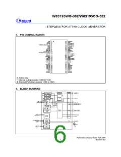
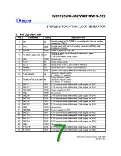
5. PIN DESCRIPTION
PIN
PIN NAME
TYPE
DESCRIPTION
Crystal output at 14.318MHz nominally with internal loading
capacitors (18pF).
1
XIN
IN
Crystal input with internal loading capacitors (18pF) and
feedback resistors.
2
3
XOUT
OUT
VDD48
PWR Power supply for USB_48
Real time input pin to change frequency to a pre-
programmed.
4
*TURBO_SEL/USB_48 I/O
3.3V USB 48Mhz clock output.
5
6
7
8
9
GND
PWR Ground pin
*PD#
IN
Power down mode
SCLK
IN
Serial clock of I2C 2-wire control interface.
Serial data of I2C 2-wire control interface.
SDATA
RESET#
I/O
OUT System reset signal when the watchdog is time out.
Dynamic output control
IN
10 &CLKREQA#
0 = active, 1 = inactive
Turbo function control.
Dynamic output control
0 = active, 1 = inactive
11 &TURBO/&CLKREQB# IN
12 SRCT7
13 SRCC7
14 VDDSRC
15 GND
OUT 0.7V current mode differential clock output for SRC
OUT 0.7V current mode differential clock output for SRC
PWR Power supply for SRC
PWR Ground pin
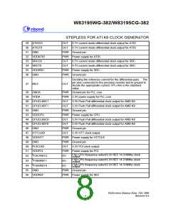
16 SRCT6
17 SRCC6
18 SRCT5
19 SRCC5
20 GND
OUT 0.7V current mode differential clock output for SRC
OUT 0.7V current mode differential clock output for SRC
OUT 0.7V current mode differential clock output for SRC
OUT 0.7V current mode differential clock output for SRC
PWR Ground pin
21 VDDSRC
22 SRCT4
23 SRCC4
24 SRCT3
25 SRCC3
26 GND
PWR Power supply for SRC
OUT 0.7V current mode differential clock output for SRC
OUT 0.7V current mode differential clock output for SRC
OUT 0.7V current mode differential clock output for SRC
OUT 0.7V current mode differential clock output for SRC
PWR Ground pin
27 ATIGT1
28 ATIGC1
OUT 0.7V current mode differential clock output for ATIG
OUT 0.7V current mode differential clock output for ATIG
Publication Release Date: Feb 2006
Revision 0.6
- 3 -

 WINBOND [ WINBOND ]