W83195WG-382/W83195CG-382
STEPLESS FOR ATI K8 CLOCK GENERATOR
Table of Content
1.
2.
3.
4.
5.
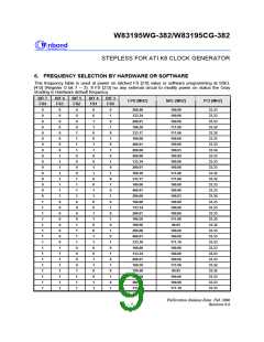
6.
7.
GENERAL DESCRIPTION ......................................................................................................... 1
PRODUCT FEATURES .............................................................................................................. 1
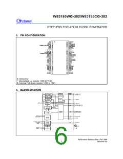
PIN CONFIGURATION............................................................................................................... 2
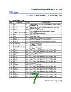
BLOCK DIAGRAM ...................................................................................................................... 2
PIN DESCRIPTION..................................................................................................................... 3
FREQUENCY SELECTION BY HARDWARE OR SOFTWARE ................................................ 5
I2C CONTROL AND STATUS REGISTERS............................................................................... 6
7.1
Register 0: ( Default : 00h )......................................................................................................6
Register 1: ( Default : XXh) ......................................................................................................6
Register 2: ( Default : 03h )......................................................................................................7
Register 3: ( Default : 03h )......................................................................................................7
Register 4: ( Default : FEh) ......................................................................................................8
Register 5: ( Default : 02h )......................................................................................................8
Register 6: ( Default : FFh )......................................................................................................9
Register 7: Winbond Chip ID – Project Code Register ( Default : 06h )...............................10
Register 8: ( Default :D0h )..................................................................................................10
Register 9: ( Default : 7Ah )....................................................................................................10
Register 10: Reserved ( Default : 3Bh ).................................................................................11
Register 11: ( Default : 0Eh )..................................................................................................11
7.2
7.3
7.4
7.5
7.6
7.7
7.8
7.9
7.10
7.11
7.12
7.13
Register 12: ( Default : XXh ).................................................................................................11
Table-2 CPU, SRC, PCI divider ratio selection Table .................................................................11
7.14
7.15
7.16
7.17
7.18
7.19
7.20
7.21
7.22
Register 13: ( Default : 3Fh )..................................................................................................12
Register 14: ( Default : D0h ) .................................................................................................12
Register 15: ( Default : 5Ch ) .................................................................................................12
Register 16: ( Default : 24h )..................................................................................................13
Register 17: Reserved ( Default : 07h ).................................................................................14
Register 18: Reserved ( Default : 7Ah ).................................................................................14
Register 19: ( Default : 04h )..................................................................................................14
Register 20: ( Default : 88h )..................................................................................................15
Register 21: ( Default : ECh ).................................................................................................15
Table3: SRC & ATIG Frequency Selection Table..............................................................................16
ACCESS INTERFACE.............................................................................................................. 17
8.
8.1
Block Write protocol ...............................................................................................................17
Publication Release Date: Feb 2006
- II -
Revision 0.6

 WINBOND [ WINBOND ]