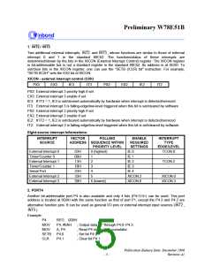
Preliminary W78E51B
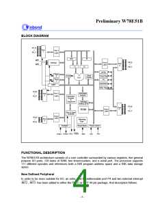
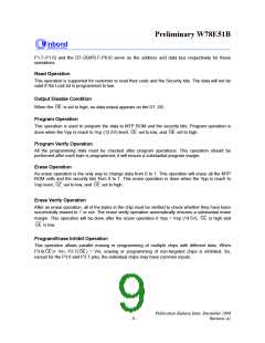
BLOCK DIAGRAM
P1.0
~
P1.7
Port
1
Port 1
Latch
ACC
B
INT2
INT3
P0.0
~
P0.7
Port 0
Latch
Interrupt
Port
0
T2
T1
DPTR
Timer
0
Stack
Pointer
PSW
Temp Reg.
PC
ALU
Timer
1
Incrementor
Addr. Reg.
UART
P3.0
~
P3.7
Port 3
Latch
Port
3
SFR RAM
Address
Instruction
Decoder
&
Sequencer
128 bytes
RAM & SFR
P2.0
~
P2.7
Port
2
Port 2
Latch
ROM
Bus & Clock
Controller
Port 4
Latch
P4.0
~
P4.3
Port
4
Watchdog
Timer
Oscillator
Reset Block
Power control
Vss
Vcc
ALE PSEN
XTAL2
XTAL1
RST
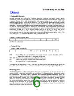
FUNCTIONAL DESCRIPTION
The W78E51B architecture consists of a core controller surrounded by various registers, five general
purpose I/O ports, 128 bytes of RAM, two timer/counters, and a serial port. The processor supports
111 different opcodes and references both a 64K program address space and a 64K data storage
space.
New Defined Peripheral
In order to be more suitable for I/O, an extra 4-bit bit-addressable port P4 and two external interrupt
INT2 , INT3 has been added to either the PLCC or QFP 44 pin package. And description follows:
- 4 -

 WINBOND [ WINBOND ]