Preliminary W78E51B
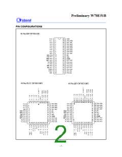
PIN DESCRIPTION
SYMBOL
DESCRIPTIONS
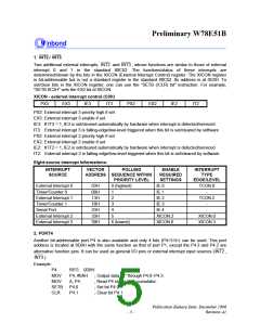
EXTERNAL ACCESS ENABLE: This pin forces the processor to execute out of
external ROM. It should be kept high to access internal ROM. The ROM address and
EA
data will not be presented on the bus if EA pin is high and the program counter is
within on-chip ROM area.
PSEN
PROGRAM STORE ENABLE: PSEN enables the external ROM data onto the Port 0
address/ data bus during fetch and MOVC operations. When internal ROM access is
performed, no PSEN strobe signal outputs from this pin.
ALE
RST
ADDRESS LATCH ENABLE: ALE is used to enable the address latch that separates
the address from the data on Port 0.
RESET: A high on this pin for two machine cycles while the oscillator is running resets
the device.
XTAL1
CRYSTAL1: This is the crystal oscillator input. This pin may be driven by an external
clock.
XTAL2
VSS
CRYSTAL2: This is the crystal oscillator output. It is the inversion of XTAL1.
GROUND: Ground potential
VDD
POWER SUPPLY: Supply voltage for operation.
PORT 0: Port 0 is a bi-directional I/O port which also provides a multiplexed low order
address/data bus during accesses to external memory. The pins of Port 0 can be
individually configured to open-drain or standard port with internal pull-ups.
P0.0- P0.7
PORT 1: Port 1 is a bi-directional I/O port with internal pull-ups. The bits have alternate
P1.0- P1.7
functions which are described below:
T2(P1.0): Timer/Counter 2 external count input
T2EX(P1.1): Timer/Counter 2 Reload/Capture control
PORT 2: Port 2 is a bi-directional I/O port with internal pull-ups. This port also provides
the upper address bits for accesses to external memory.
P2.0- P2.7
P3.0- P3.7
PORT 3: Port 3 is a bi-directional I/O port with internal pull-ups. All bits have alternate
functions, which are described below:
RXD(P3.0) : Serial Port receiver input
TXD(P3.1) : Serial Port transmitter output
INT0 (P3.2) : External Interrupt 0
INT1(P3.3) : External Interrupt 1
T0(P3.4) : Timer 0 External Input
T1(P3.5) : Timer 1 External Input
WR (P3.6) : External Data Memory Write Strobe
RD(P3.7) : External Data Memory Read Strobe
PORT 4: Another bit-addressable bidirectional I/O port P4. P4.3 and P4.2 are
P4.0- P4.3
alternative function pins. It can be used as general I/O port or external interrupt input
sources (INT2 /INT3 ).
Publication Release Date: December 1998
- 3 -
Revision A1

 WINBOND [ WINBOND ]