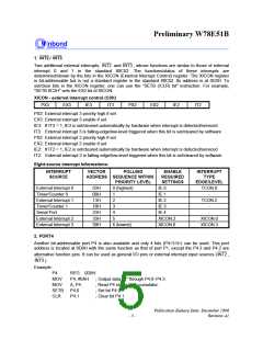
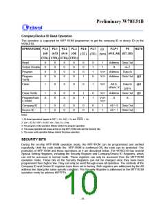
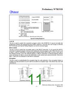
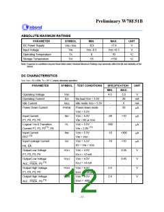
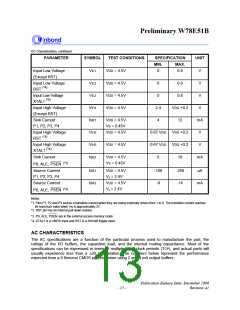
Preliminary W78E51B
P1.7- P1.0) and the D7- D0(P0.7- P0.0) serve as the address and data bus respectively for these
operations.
Read Operation
This operation is supported for customer to read their code and the Security bits. The data will not be
valid if the Lock bit is programmed to low.
Output Disable Condition
When the OE is set to high, no data output appears on the D7..D0.
Program Operation
This operation is used to program the data to MTP ROM and the security bits. Program operation is
done when the Vpp is reach to Vcp (12.5V) level, CE set to low, and OE set to high.
Program Verify Operation
All the programming data must be checked after program operations. This operation should be
performed after each byte is programmed; it will ensure a substantial program margin.
Erase Operation
An erase operation is the only way to change data from 0 to 1. This operation will erase all the MTP
ROM cells and the security bits from 0 to 1. This erase operation is done when the Vpp is reach to
Vep level, CE set to low, and OE set to high.
Erase Verify Operation
After an erase operation, all of the bytes in the chip must be verified to check whether they have been
successfully erased to 1 or not. The erase verify operation automatically ensures a substantial erase
margin. This operation will be done after the erase operation if Vpp = Vep (14.5V), CE is high and
OE is low.
Program/Erase Inhibit Operation
This operation allows parallel erasing or programming of multiple chips with different data. When
P3.6(CE)= VIH, P3.7( OE ) = VIH, erasing or programming of non-targeted chips is inhibited. So,
except for the P3.6 and P3.7 pins, the individual chips may have common inputs.
Publication Release Date: December 1998
- 9 -
Revision A1

 WINBOND [ WINBOND ]