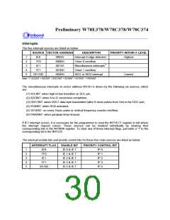
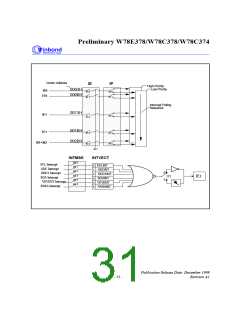
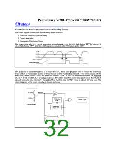
Preliminary W78E378/W78C378/W78C374
Appendix A. Application Note for Usage of ADC
To use the ADC, users should pay attention to the following points:
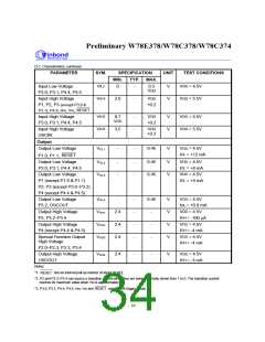
DD
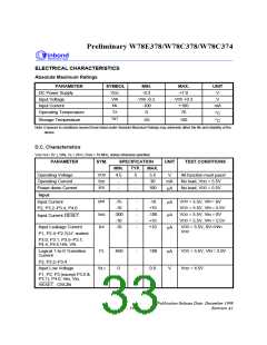
(1) According to the absolute maximum ratings, the input voltage should not exceed V
+0.3V,
DD
-
-
especially for the ADC channel pins (P2.4 P2.7 & P3.5 P3.7). If a voltage over V +0.3V exists
on any of these ADC channel pins, the AD conversion will fail.
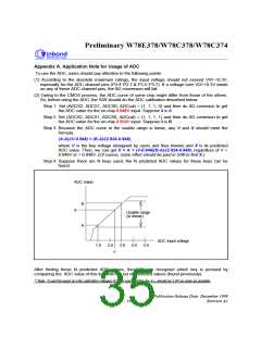
(2) Owing to the CMOS process, the ADC curve of some chip might differ from those of the others.
So, before using the ADC, the S/W should do the ADC calibration described below.
Step 1. Set (ADCS2, ADCS1, ADCS0, ADCcal) = (1, 1, 1, 0) and then do AD coversion to get
0.948V
A
the ADC value for the on-chip
Step 2. Set (ADCS2, ADCS1, ADCS0, ADCcal) = (1, 1, 1, 1) and then do AD coversion to get
2.924V
input. Suppose it is
.
B
input. Suppose it is .
the ADC value for the on-chip
Step 3. Because the ADC curve in the usable range is linear, any V and X should meet the
formula:
(X-A)/(V-0.948) = (B-A)/(2.924-0.948),
where V is the key voltage (designed by users and thus known) and X is its predicted
ADC value. Then, we can get X = A + (V-0.948)(B-A)/(2.924-0.948), regardless of V >
Of course, some effort should be paid in S/W to find .)
0.948V or < 0.948V. (
X
Step 4. Suppose there are N keys used, the N predicted ADC values for these keys can be
found.
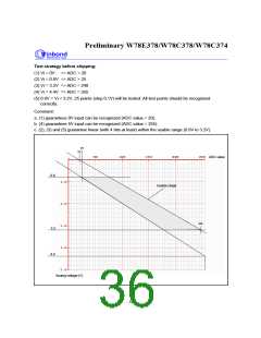
ADC value
B
X
Usable range
(is linear)
A
ADC input voltage
1.0
2.0
3.0
4.0
5.0
V
After finding these N predicted ADC values, the S/W can recognize which key is pressed by
comparing the ADC value of this key with the set of predicted values (found previously).
** Note: To get the exact on-chip calibration voltages (0.948V and 2.924V), the VDD should be 5.0V as close as possible.
Publication Release Date: December 1999
- 35 -
Revision A1

 WINBOND [ WINBOND ]