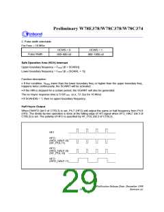
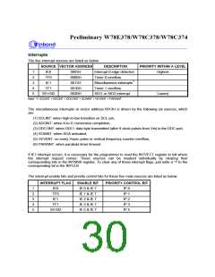
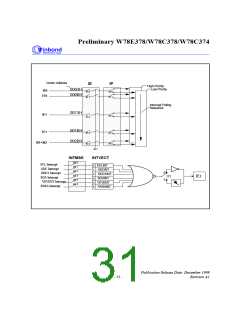
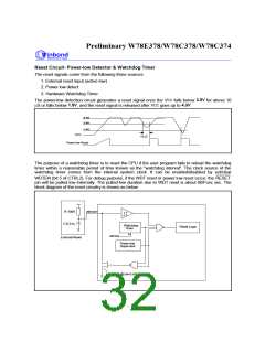
Preliminary W78E378/W78C378/W78C374
ELECTRICAL CHARACTERISTICS
Absolute Maximum Ratings
PARAMETER
DC Power Supply
Input Voltage
SYMBOL
MIN.
-0.3
SS
MAX.
+7.0
DD
UNIT
V
DD
V
IN
V
V
-0.3
V
+0.3
V
IN
Input Current
I
-100
0
+100
70
mA
A
T
Operating Temperature
°C
TST
Storage Temperature
-55
150
°
C
Note: Exposure to conditions beyond those listed under Absolute Maximum Ratings may adversely affect the life and reliability of the
device.
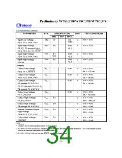
D.C. Characteristics
VDD-VSS= 5V 10%, TA = 25 C, Fosc = 10 MHz, unless otherwise specified.
±
°
PARAMETER
SYM.
SPECIFICATION
MIN. TYP. MAX.
UNIT
TEST CONDITIONS
DD
Operating Voltage
Operating Current
Power-down Current
Input
V
4.5
5
-
5.5
30
V
All function must pass!
DD
DD
I
-
-
mA
No load, V = 5.5V
PD
DD
I
-
100
No load, V = 5.5V
m
A
IN1
DD
DD
IN
Input Current
I
-75
-10
-
-10
+10
-100
+10
+10
V
V
V
V
= 5.5V, V = 0V
m
A
IN
-
-
-
-
= 5.5V, V = 5.5V
-
P2, P3.2 P3.4, P4.0
IN2
DD
DD
DD
IN
I
-300
-10
= 5.5V, V = 0V
m
A
RESET
Input Current
IN
= 5.5V, V = 5.5V
LK
IN
Input Leakage Current
I
-10
V
V
= 5.5V, 0V<V <
mA
DD
S.F. enabled)
-
P1, P2.4 P2.7(
-
P3.0, P3.1, P3.5 P3.7,
IN
IN
P4.4, P4.5 H , V
TL
DD
IN
Logical 1-to-0 Transition
Current
I
-650
0
-
-100
0.8
V
V
= 5.5V, V = 2.0V
m
A
-
P2, P3.2 P3.4
IL1
V
DD
Input Low Voltage
-
V
= 4.5V
P1, P2, P3 (except P3.0 &
IN
IN
P3.1), P4.0, H , V ,
RESET
, OSCIN
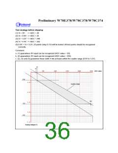
Publication Release Date: December 1999
Revision A1
- 33 -

 WINBOND [ WINBOND ]