Preliminary W78E378/W78C378/W78C374
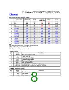
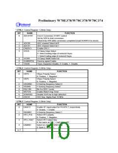
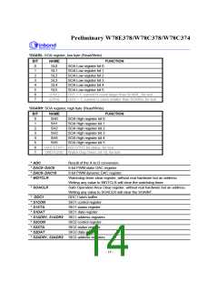
* CTRL1: Control Register 1 (Write Only)
BIT
NAME
FUNCTION
A-to-D Conversion START control
0
ADCSTRT
Set by S/W to start conversion.
Cleared by H/W while conversion completed (read SOARH.6 to check).
ADC channel Select bit 0
1
2
3
4
ADCS0
ADCS1
ENDDC1
HCES
ADC channel Select bit 1
Enable DDC1
H-Clamp Edge Select
0: Select leading edge of restored Hsync
1: Select trailing edge of restored Hsync
H-Clamp Width Select bit
5
6
7
HCWS
DUMMYEN
VSDIS
Dummy signal Enable
Vsync Separator Disable, 0: Enable, 1: Disable
* CTRL2: Control Register 2 (Write Only)
BIT
NAME
HSPS
FUNCTION
0
HSync Polarity Select
0: Positive, 1: Negative
VSync Polarity Select
0: Positive, 1: Negative
1
VSPS
2
3
4
5
6
7
HDUMS0
VDUMS
DDC1B9
WDTEN
SOAHDIS
OSCHI
H Dummy frequency Select 0
V Dummy frequency Select
Bit 9 in DDC1 mode
Enable Watch Dog Timer
Disable SOA low to high detection
OSC freq. Higher than 10 MHz
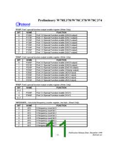
* CTRL3: Control Register 3 (Write Only)
BIT
NAME
ENHFO
FUNCTION
Enable HF input/output for P4.0/P4.7, respectively
0: Disable, 1: Enable
0
1
2
HDUMS1
H Dummy frequency Select 1
Select HFO polarity
HFO_POL
0: Positive, 1: Negative
3
4
HFO_HALF
Select HFO output freq.
0: the same as HFI, 1: half of the HFI
Select on-chip ext. RAM bank
0: Bank 0, 1: Bank 1
ENBNK1
-
-
-
5 7
- 10 -

 WINBOND [ WINBOND ]