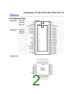
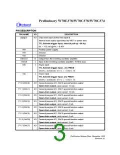
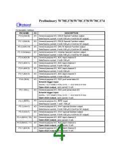
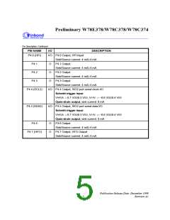
Preliminary W78E378/W78C378/W78C374
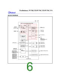
BLOCK DIAGRAM
VDD
VSS
80C31 Core excluding internal RAM
freq2
Note:
freq1 = freq2
CPU
freq1
OSCIN
Osc.
Circuit
Interrupt
Processor
INT0 (P3.2)
OSCOUT
T0 (P3.5)
T1 (P3.6)
Timer 0
Timer 1
RESET
Reset
Circuit
P1, P2, P3
P4
I/O Port
Power Low
Detection
Note:
P1, P4.4~P4.5
P3.0~P3.1 & P3.5~P3.7
are open-drain.
Watch Dog
Timer
SCL (P3.1)
SDA (P3.0)
VPP (P3.2)
Program Memory
SIO1
SIO2
Data Memory
RAM: 576 Bytes
SCL2 (P4.4)
SDA2 (P4.5)
HIN, VIN
HFI (P4.0)
Sync.
Processor
VOUT (P3.4)
HOUT (P3.3)
Hclamp (P2.3)
HFO (P4.7)
DAC0~7 (P1.0~P1.7)
DAC8~10 (P2.0~P2.2)
Static DACs
ADC0 (P2.4)
ADC1 (P2.5)
ADC2 (P2.6)
ADC3 (P2.7)
ADC4 (P3.5)
ADC5 (P3.6)
ADC6 (P3.7)
Dynamic DACs
ADC
8-bit Internal Bus
- 6 -

 WINBOND [ WINBOND ]