Preliminary W78E378/W78C378/W78C374
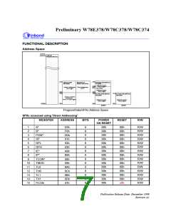
SFRs accessed using 'Direct Addressing', continued
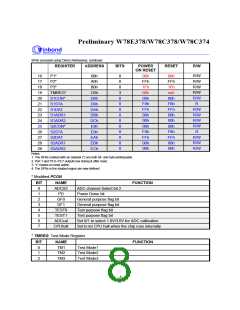
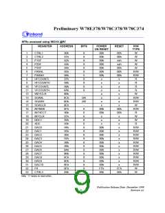
REGISTER
ADDRESS
BITS
POWER
RESET
R/W
ON RESET
R/W
R/W
R/W
R/W
R/W
R
16
17
18
19
20
21
22
23
24
25
26
27
28
28
P1*
90h
A0h
B0h
C0h
D8h
D9h
DAh
DBh
DCh
E8h
E9h
EAh
EBh
ECh
8
8
8
3
8
8
8
8
8
8
8
8
8
8
00h
FFh
1Fh
00h
00h
F8h
FFh
00h
00h
00h
F8h
FFh
00h
00h
00h
FFh
1Fh
xxh
00h
F8h
FFh
00h
00h
00h
F8h
FFh
00h
00h
P2*
P3*
TMREG*
S1CON*
S1STA
S1DAT
S1ADR1
S1ADR2
S2CON*
S2STA
S2DAT
S2ADR1
S2ADR2
R/W
R/W
R/W
R/W
R
R/W
R/W
R/W
Notes:
1. The SFRs marked with an asterisk (*) are both bit- and byte-addressable.
2. Port 1 and P3.5 P3.7 outputs low during & after reset.
-
3. "x" means no reset action.
4. The SFRs in the shaded region are new-defined.
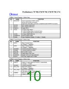
* Modified PCON
BIT
0
NAME
ADCS2
PD
FUNCTION
ADC channel Select bit 2
Power Down bit
1
2
GF0
General purpose flag bit
General purpose flag bit
Test purpose flag bit
Test purpose flag bit
3
GF1
4
TEST0
TEST1
ADCcal
CPUhalt
5
6
Set 0/1 to select 1.0V/3.0V for ADC calibration
Set to let CPU halt when the chip runs internally
7
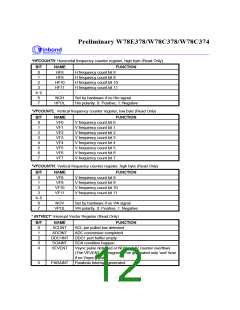
* TMREG: Test Mode Register
BIT
0
NAME
TM1
FUNCTION
Test Mode1
Test Mode2
Test Mode3
1
TM2
2
TM3
- 8 -

 WINBOND [ WINBOND ]