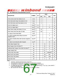
W25Q16DV
8.3 Power-Up Power-Down Timing and Requirements
SPEC
PARAMETER
SYMBOL
UNIT
MIN
20
5
MAX
VCC (min) to /CS Low
tVSL(1)
tPUW(1)
VWI(1)
µs
ms
V
Time Delay Before Write Instruction
Write Inhibit Threshold Voltage
1.0
2.0
Note:
1. These parameters are characterized only.
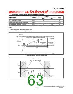
VCC
VCC (max)
Program, Erase and Write Instructions are ignored
/CS must track VCC
VCC (min)
Read Instructions
Allowed
Device is fully
Accessible
tVSL
Reset
State
VWI
tPUW
Time
Figure 39a. Power-up Timing and Voltage Levels
/CS must track VCC
during VCC Ramp Up/Down
VCC
/CS
Time
Figure 39b. Power-up, Power-Down Requirement
Publication Release Date: October 29, 2012
Revision D
- 63 -

 WINBOND [ WINBOND ]