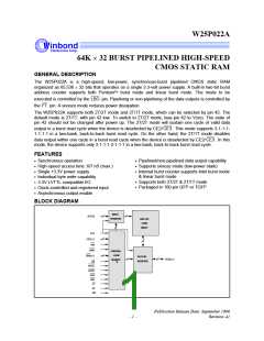
W25P022A
FUNCTIONAL DESCRIPTION
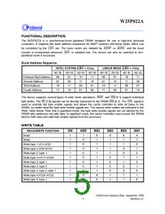
The W25P022A is a synchronous-burst pipelined SRAM designed for use in high-end personal
computers. It supports two burst address sequences for Intelä systems and linear mode, which can
be controlled by the LBO pin. The burst cycles are initiated by ADSP or ADSC and the burst
counter is incremented whenever ADV is sampled low. The device can also be switched to non-
pipelined mode if necessary.
Burst Address Sequence
INTEL SYSTEM (LBO = VDDQ)
LINEAR MODE (LBO = VSSQ)
A[1:0]
00
A[1:0]
01
A[1:0]
10
A[1:0]
11
A[1:0]
00
A[1:0]
01
A[1:0]
10
A[1:0]
11
External Start Address
Second Address
Third Address
01
00
11
10
01
10
11
00
10
11
00
01
10
11
00
01
Fourth Address
11
10
01
00
11
00
01
10
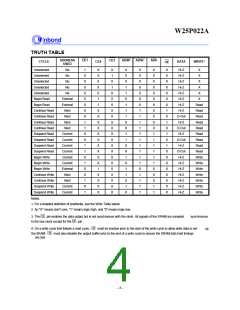
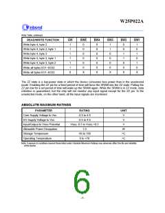
The device supports several types of write mode operations. BWE and BW [4:1] support individual
byte writes. The BE [7:0] signals can be directly connected to the SRAM BW [4:1]. The GW signal is
used to override the byte enable signals and allows the cache controller to write all bytes to the
SRAM, no matter what the byte write enable signals are. The various write modes are indicated in the
Write Table below. Note that in pipelined mode, the byte write enable signals are not latched by the
SRAM with addresses but with data. In pipelined mode, the cache controller must ensure the SRAM
latches both data and valid byte enable signals from the processor.
WRITE TABLE
READ/WRITE FUNCTION
Read
GW
1
BWE
BW4
X
1
BW3
X
1
BW2
X
1
BW1
X
1
1
0
0
0
0
0
0
0
0
0
0
Read
1
1
1
1
1
0
Write byte 1 I/O1- I/O8
Write byte 2 I/O9- I/O16
Write byte 2, byte 1
Write byte 3 I/O17- I/O24
Write byte 3, byte 1
Write byte 3, byte 2
Write byte 3, byte 2, byte 1
Write byte 4 I/O25- I/O32
Write byte 4, byte 1
1
1
1
0
1
1
1
1
0
0
1
1
0
1
1
1
1
0
1
0
1
1
0
0
1
1
1
0
0
0
1
0
1
1
1
1
0
1
1
0
Publication Release Date: September 1996
Revision A1
- 5 -

 WINBOND [ WINBOND ]