W25P022A
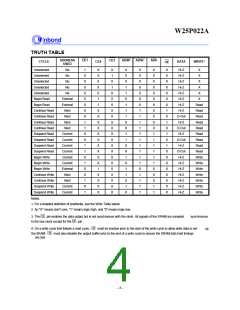
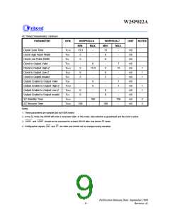
TRUTH TABLE
ADDRESS
USED
CE1
CE3
ADSP
ADSC
ADV
CYCLE
CE2
DATA
WRITE*
OE
Unselected
No
1
0
0
0
0
0
0
X
X
1
1
X
X
1
1
X
1
0
X
1
X
1
X
X
0
X
1
X
0
0
1
1
0
1
1
1
X
X
1
1
X
X
1
X
1
1
X
1
X
0
X
X
0
0
X
0
1
1
1
1
1
1
1
1
1
1
0
1
1
1
1
X
X
X
X
X
X
X
0
0
0
0
1
1
1
1
1
1
X
0
0
1
1
X
X
X
X
X
X
X
1
Hi-Z
Hi-Z
Hi-Z
Hi-Z
Hi-Z
Hi-Z
Hi-Z
Hi-Z
D-Out
Hi-Z
D-Out
Hi-Z
D-Out
Hi-Z
D-Out
Hi-Z
Hi-Z
Hi-Z
Hi-Z
Hi-Z
Hi-Z
Hi-Z
X
Unselected
No
X
Unselected
No
X
1
X
Unselected
No
X
0
X
Unselected
No
X
0
X
Begin Read
External
External
Next
1
X
Begin Read
1
0
Read
Read
Read
Read
Read
Read
Read
Read
Read
Write
Write
Write
Write
Write
Write
Write
Continue Read
Continue Read
Continue Read
Continue Read
Suspend Read
Suspend Read
Suspend Read
Suspend Read
Begin Write
X
X
X
X
X
X
X
X
X
X
1
X
X
X
X
X
X
X
X
X
X
0
Next
0
Next
1
Next
0
Current
Current
Current
Current
Current
Current
External
Next
1
0
1
0
X
X
X
X
X
X
X
Begin Write
Begin Write
Continue Write
Continue Write
Suspend Write
Suspend Write
X
X
X
X
X
X
X
X
Next
Current
Current
Notes:
1. For a detailed definition of read/write, see the Write Table below.
2. An "X" means don't care, "1" means logic high, and "0" means logic low.
3. The OE pin enables the data output but is not synchronous with the clock. All signals of the SRAM are sampled
to the bus clock except for the OE pin.
synchronous
4. On a write cycle that follows a read cycle, OE must be inactive prior to the start of the write cycle to allow write data to set
up
the SRAM. OE must also disable the output buffer prior to the end of a write cycle to ensure the SRAM data hold timings
are met.
- 4 -

 WINBOND [ WINBOND ]