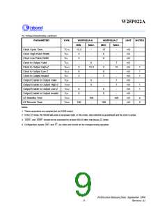
W25P022A
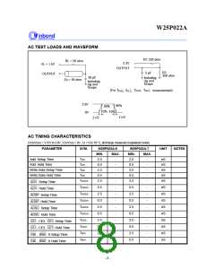
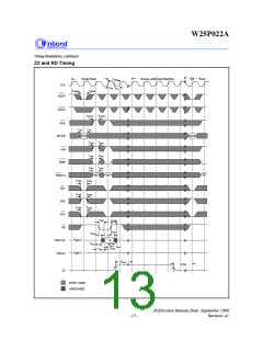
AC Timing Characteristics, continued
PARAMETER
SYM.
W25P022A-6
MIN. MAX.
13.3
W25P022A-7
MIN. MAX.
15
UNIT
NOTES
Clock Cycle Time
TCYC
TKH
-
-
nS
nS
nS
nS
nS
nS
nS
nS
nS
nS
nS
nS
nS
Clock High Pulsh Width
Clock Low Pulse Width
Clock to Output Valid
5
5
-
6
6
-
TKL
-
-
7
TKQ
-
6
-
Clock to Output High-Z
Clock to Output Low-Z
Clock to Output Invalid
Output Enable to Output Valid
Output Enable to Output High-Z
Output Enable to Output Low-Z
Output Enable to Output Invalid
ZZ Standby Time
TKHZ
TKLZ
TKX
2
13.3
2
15
-
1
1
1
0
-
0
2
-
2
-
TOE
-
6
-
7
TOHZ
TOLZ
TOX
-
6
-
7
1
1
0
-
0
-
0
-
100
-
0
-
TZZS
TZZR
-
-
100
-
2
3
ZZ Recover Time
100
100
Notes:
1. These parameters are sampled but not 100% tested
2. In the ZZ mode, the SRAM will enter a low-power state. In this mode, data retention is guaranteed and the clock is active.
3. ADSC and ADSP should not be accessed for at least 100 nS after chip leaves ZZ mode.
4. Configuration signals LBO and FT are static and should not be changed during operation.
Publication Release Date: September 1996
- 9 -
Revision A1

 WINBOND [ WINBOND ]