W25P022A
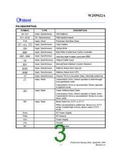
PIN DESCRIPTION
SYMBOL
TYPE
DESCRIPTION
Input, Synchronous
I/O, Synchronous
Input, Clock
Host Address
A0- A15
I/O1- I/O32
CLK
Data Inputs/Outputs
Processor Host Bus Clock
Chip Enables
Input, Synchronous
CE1, CE2, CE3
GW
Input, Synchronous
Input, Synchronous
Input, Synchronous
Global Write
Byte Write Enable from Cache Controller
BWE
BW1- BW4
Host Bus Byte Enables used with BWE
Input, Asynchronous Output Enable Input
OE
ADV
Input, Synchronous
Input, Synchronous
Input, Synchronous
Internal Burst Address Counter Advance
Address Status from chip set
Address Status from CPU
ADSC
ADSP
ZZ
Input, Asynchronous Snooze Pin for Low-power State, internally pulled low
Input, Static
Input, Static
Input, Static
Connected to VSSQ: Device operates in flow-through
(non-pipelined) mode.
FT
Connected to VDDQ or unconnected: Device operates
in piplined mode.
Lower Address Burst Order
LBO
MS
Connected to VSSQ: Device operates in linear mode.
Connected to VDDQ or unconnected: Device is in non-
linear mode.
Mode Select for 2T/2T or 2T/1T
When unconnected or pulled low, device is in 2T/1T
mode; if pulled high (VDDQ), device enters 2T/2T
mode.
VDDQ
VSSQ
VDD
VSS
I/O Power Supply
I/O Ground
Power Supply
Ground
NC
No Connection
Publication Release Date: September 1996
- 3 -
Revision A1

 WINBOND [ WINBOND ]