I5216 SERIES
Advanced Information
PRELIMINARY
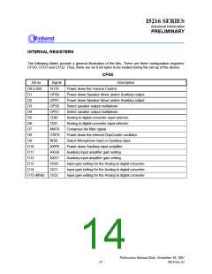
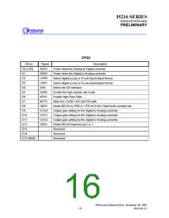
CFG2
Bit no.
D0 (LSB)
D1
Signal
ADPD
DAPD
LAW0
LAW1
I2S0
Description
Power down the Analog to Digital converter
Power down the Digital to Analog converter
Select digital µ-Law or A-Law input/output format
Select digital µ-Law or A-Law input/output format
Select the I2S interface
D2
D3
D4
D5
HSR0
HPF0
MUTE
CKDV
COG0
COG1
COG2
CKD2
-
Enable the high sample rate mode
Enable High Pass Filter
D6
D7
Mute the CODEC A/D and D/A path
D8
Divide MCLK by 2560 or 1728 for 8 kHz ChipCorder sample rate
Output gain setting for the Digital to Analog converter
Output gain setting for the Digital to Analog converter
Output gain setting for the Digital to Analog converter
Divide MCLK frequency by 2 or 1
Reserved
D9
D10
D11
D12
D13
D14
D15 (MSB)
-
Reserved
-
Reserved
Publication Release Date: November 30, 2001
Revision A1
-16

 WINBOND [ WINBOND ]