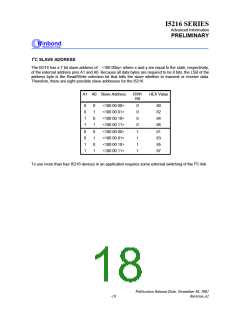
I5216 SERIES
Advanced Information
PRELIMINARY
INTERNAL REGISTERS
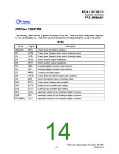
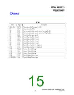
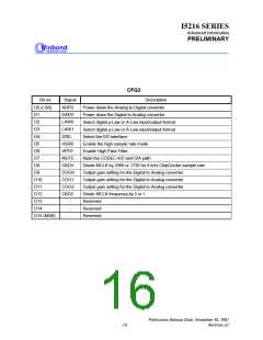
The following tables provide a general illustration of the bits. There are three configuration registers:
CFG0, CFG1 and CFG2. Thus, there are six 8-bit bytes to be loaded during the set-up of the device.
CFG0
Bit no.
D0 (LSB)
D1
Signal
VLPD
OPA0
OPA1
OPS0
OPS1
CDI0
Description
Power down the Volume Control.
Power down Speaker driver and/or Auxiliary output.
Power down Speaker driver and/or Auxiliary output.
Select speaker output multiplexer.
D2
D3
D4
Select speaker output multiplexer.
D5
Analog to digital converter input selector.
Analog to digital converter input selector.
Compress the filter signal.
D6
CDI1
D7
AMT0
OSPD
INS0
D8
Power down the internal ChipCorder oscillator.
Select Microphone input or Auxiliary input.
Power down Auxiliary input amplifier.
D9
D10
D11
D12
D13
D14
D15 (MSB)
AXPD
AXG0
AXG1
CIG0
Auxiliary input amplifier gain setting.
Auxiliary input amplifier gain setting.
Input gain setting for the Analog to digital converter.
Input gain setting for the Analog to digital converter.
Input gain setting for the Analog to digital converter.
CIG1
CIG2
Publication Release Date: November 30, 2001
Revision A1
-14

 WINBOND [ WINBOND ]