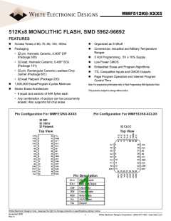
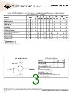
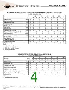
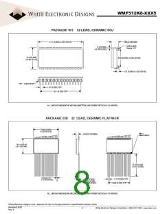
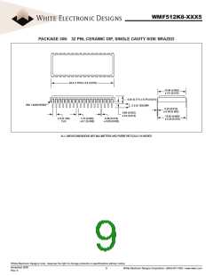
WMF512K8-XXX5
White Electronic Designs
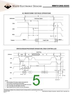
AC WAVEFORMS FOR READ OPERATIONS
tRC
Addresses
CS#
Addresses Stable
tACC
tDF
tOE
OE#
WE#
tCE
tOH
High Z
High Z
Outputs
Output Valid
WRITE/ERASE/PROGRAM OPERATION, WE# CONTROLLED
Data# Polling
Addresses
5555H
PA
PA
t
WC
tAH
tRC
tAS
CS#
OE#
WE#
t
GHWL
tWP
tWHWH1
tWPH
t
CS
tDF
tDH
tOE
A0H
PD
I/OOUT
I/O7#
Data
tDS
tOH
5.0 V
tCE
NOTES:
1. PA is the address of the memory location to be programmed.
2. PD is the data to be programmed at byte address.
3. I/O7# is the output of the complement of the data written to the device.
4. I/OOUT is the output of the data written to the device.
5. Figure indicates last two bus cycles of four bus cycle sequence.
White Electronic Designs Corp. reserves the right to change products or specifications without notice.
November 2005
Rev. 6
5
White Electronic Designs Corporation • (602) 437-1520 • www.wedc.com

 WEDC [ WHITE ELECTRONIC DESIGNS CORPORATION ]