WMF512K8-XXX5
White Electronic Designs
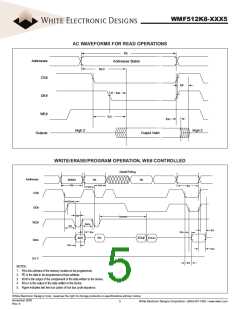
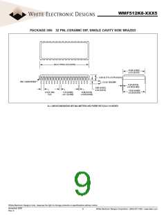
ALTERNATE CS# CONTROLLED PROGRAMMING OPERATION TIMINGS
Data# Polling
Addresses
WE#
5555H
tWC
PA
PA
tAH
tAS
tGHEL
OE#
CS#
tCP
tWHWH1
tCPH
tDH
tWS
I/O7#
A0H
PD
I/OOUT
Data
tDS
5.0 V
Notes:
1. PA represents the address of the memory location to be programmed.
2. PD represents the data to be programmed at byte address.
3. I/O7# is the output of the complement of the data written to the device.
4. I/OOUT is the output of the data written to the device.
5. Figure indicates the last two bus cycles of a four bus cycle sequence.
White Electronic Designs Corp. reserves the right to change products or specifications without notice.
November 2005
Rev. 6
7
White Electronic Designs Corporation • (602) 437-1520 • www.wedc.com

 WEDC [ WHITE ELECTRONIC DESIGNS CORPORATION ]