WMF512K8-XXX5
White Electronic Designs
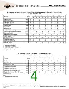
AC CHARACTERISTICS – WRITE/ERASE/PROGRAM OPERATIONS, WE# CONTROLLED
VCC = 5.0V, -55°C ≤ TA ≤ +125°C
-60
-70
-90
-120
-150
Parameter
Symbol
tAVAV tWC
Unit
Min Max Min Max Min Max Min Max Min Max
Write Cycle Time
60
0
40
0
70
0
45
0
90
0
45
0
120
0
150
0
ns
ns
ns
Chip Select Setup Time
Write Enable Pulse Width
Address Setup Time
tELWL
tWLWH
tAVWH
tCS
tWP
tAS
50
0
50
0
ns
Data Setup Time
Data Hold Time
Address Hold Time
tDVWH
tWHDX
tWHAX
tWHWL
tWHWH1
tWHWH2
tGHWL
tDS
tDH
tAH
40
0
40
20
45
0
45
20
45
0
45
20
50
0
50
20
50
0
50
20
ns
ns
ns
ns
µs
sec
ms
µs
sec
ns
Write Enable Pulse Width High
Duration of Byte Programming Operation (1)
Sector Erase Time (2)
Read Recovery Time before Write
VCC Set-up Time
Chip Programming Time
Output Enable Setup Time
Output Enable Hold Time (4)
Chip Erase Time (3)
tWPH
300
15
300
15
300
15
300
15
300
15
0
50
0
50
0
50
0
50
0
50
tVCS
11
64
11
64
11
64
11
64
11
64
tOES
tOEH
0
10
0
10
0
10
0
10
0
10
ns
sec
NOTES:
1. Typical value for tWHWH1 is 7µs.
2. Typical value for tWHWH2 is 1sec.
3. Typical value for Chip Erase time is 8sec.
4. For Toggle and Data# Polling.
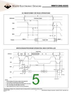
AC CHARACTERISTICS – READ ONLY OPERATIONS
VCC = 5.0V, -55°C ≤ TA ≤ +125°C
-60
-70
-90
-120
-150
Unit
Parameter
Symbol
Min Max Min Max Min Max Min Max Min Max
60 70 90 120 150
Read Cycle Time
tAVAV
tRC
tACC
tCE
tOE
tDF
ns
ns
ns
ns
ns
ns
ns
Address Access Time
tAVQV
tELQV
tGLQV
tEHQZ
tGHQZ
tAXQX
60
60
35
20
20
70
70
35
20
20
90
90
35
20
20
120
120
50
150
150
55
Chip Select Access Time
Output Enable to Output Valid
Chip Select to Output High Z (1)
Output Enable High to Output High Z (1)
30
35
tDF
30
35
Output Hold from Address, CS# or OE# Change,
whichever is First
tOH
0
0
0
0
0
NOTES:
1. Guaranteed by design, but not tested
White Electronic Designs Corp. reserves the right to change products or specifications without notice.
November 2005
Rev. 6
4
White Electronic Designs Corporation • (602) 437-1520 • www.wedc.com

 WEDC [ WHITE ELECTRONIC DESIGNS CORPORATION ]