WMF512K8-XXX5
White Electronic Designs
ABSOLUTE MAXIMUM RATINGS (1)
RECOMMENDED OPERATING CONDITIONS
Parameter
Operating Temperature
Supply Voltage (VCC) (1)
Unit
°C
V
V
°C
Parameter
Supply Voltage
Symbol
VCC
VIH
VIL
TA
Min
4.5
2.0
-0.5
-55
-40
11.5
Max
5.5
VCC + 0.5
+0.8
+125
+85
12.5
Unit
V
V
-55 to +125
-2.0 to +7.0
-2.0 to +7.0
-65 to +150
+300
Input High Voltage
Input Low Voltage
Operating Temp. (Mil.)
Operating Temp. (Ind.)
A9 Voltage for Sector Protect
Signal Voltage Range(any pin except A9) (2)
Storage Temperature Range
Lead Temperature (soldering, 10 seconds)
Data Retention Mil Temp
Endurance - erase/program cycles (Mil Temp)
A9 Voltage for sector protect (VID) (3)
NOTES:
1. Stresses above the absolute maximum rating may cause permanent damage to the
device. Extended operation at the maximum levels may degrade performance and
affect reliability.
2. Minimum DC voltage on input or I/O pins is -0.5V. During voltage transitions, inputs
may overshoot VSS to -2.0 V for periods of up to 20ns. Maximum DC voltage on
output and I/O pins is VCC + 0.5V. During voltage transitions, outputs may overshoot
to Vcc + 2.0 V for periods of up to 20ns.
V
°C
°C
V
°C
TA
VID
20
years
cycles
V
100,000 min
-2.0 to +14.0
CAPACITANCE
TA = +25°C
Parameter
Symbol
Conditions
Max Unit
Address Input capacitance
Output Enable capacitance
Write Enable capacitance
Chip Select capacitance
Data I/O capacitance
CAD VI/O = 0 V, f = 1.0 MHz 15 pF
COE VIN = 0 V, f = 1.0 MHz 15 pF
CWE VIN = 0 V, f = 1.0 MHz 15 pF
CCS VIN = 0 V, f = 1.0 MHz 15 pF
CI/O VI/O = 0 V, f = 1.0 MHz 15 pF
3. Minimum DC input voltage on A9 pin is -0.5V. During voltage transitions, A9 may
overshoot Vss to -2V for periods of up to 20ns. Maximum DC input voltage on A9 is
+13.5V which may overshoot to 14.0 V for periods up to 20ns.
This parameter is guaranteed by design but not tested.
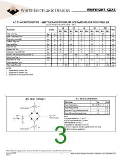
DC CHARACTERISTICS — CMOS COMPATIBLE
VCC = 5.0V, VSS = 0V, -55°C ≤ TA ≤ +125°C
Parameter
Symbol
ILI
Conditions
Min
Max
10
10
50
60
Unit
µA
µA
mA
mA
mA
V
Input Leakage Current
Output Leakage Current
VCC Active Current for Read (1)
VCC = 5.5, VIN = GND to VCC
VCC = 5.5, VIN = GND to VCC
CS# = VIL, OE# = VIH, f = 5MHz
CS# = VIL, OE# = VIH
VCC = 5.5, CS# = VIH, f = 5MHz
IOL = 8.0 mA, VCC = 4.5
ILOx32
ICC1
ICC2
ICC4
VOL
VCC Active Current for Program or Erase (2)
VCC Standby Current
Output Low Voltage
Output High Voltage
Low VCC Lock-Out Voltage
NOTES:
1.6
0.45
VOH1
VLKO
IOH = -2.5 mA, VCC = 4.5
0.85 x VCC
3.2
V
V
4.2
1. The ICC current listed includes both the DC operating current and the frequency dependent component (at 5 MHz).
The frequency component typically is less than 2 mA/MHz, with OE# at VIH
CC active while Embedded Algorithm (program or erase) is in progress.
3. DC test conditions: VIL = 0.3V, VIH = VCC - 0.3V
.
2.
I
White Electronic Designs Corp. reserves the right to change products or specifications without notice.
November 2005
Rev. 6
2
White Electronic Designs Corporation • (602) 437-1520 • www.wedc.com

 WEDC [ WHITE ELECTRONIC DESIGNS CORPORATION ]