Preliminary
VG37648041AT
256M:x4, x8, x16
VIS
CMOS Synchronous Dynamic RAM
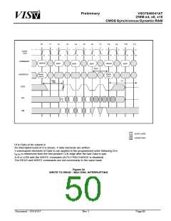
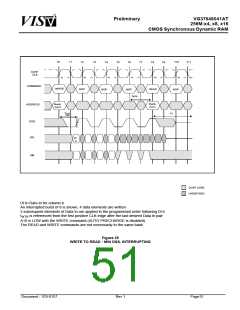
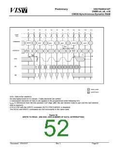
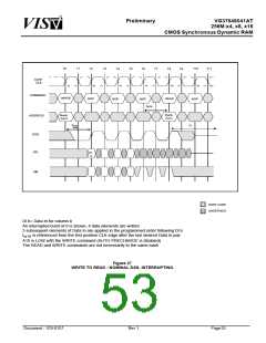
T0
T1
T10
T2
T3
T4
T5
T6
T7
T9
T11
T8
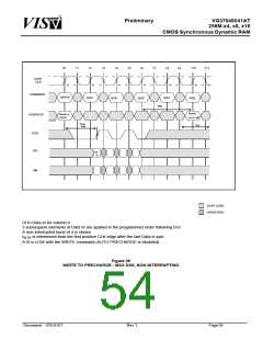
CLK#
CLK
COMMAND
ADDRESS
WRITE
NOP
READ
NOP
NOP
NOP
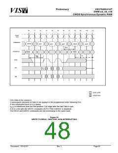
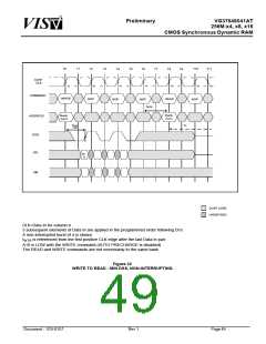
tWTR
Bank,
Col n
Bank,
Col b
tDSS
max
CL
DQS
DQ
Dl
b
DM
DONT’ CARE
UNDEFINED
Dl b=Data In for column b
An interrupted burst of 8 is shown, 4 data elements are written
3 subsequent elements of Data In are applied in the programmed order following Dl b
tWTR is referenced from the first positive CLK edge after the last Data In pair
A10 is LOW with the WRITE command (AUTO PRECHARGE is disabled)
The READ and WRITE commands are not necessarily to the same bank
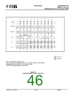
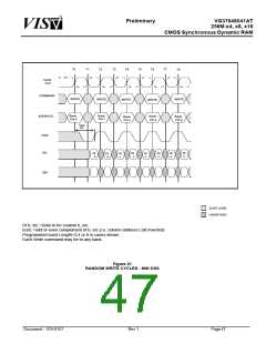
Figure 24
WRITE TO READ - MAX DSS, INTERRUPTING
Document : 1G5-0157
Rev.1
Page50

 VML [ VANGUARD INTERNATIONAL SEMICONDUCTOR ]