VITESSE
SEMICONDUCTOR CORPORATION
Data Sheet
10-Bit Transceiver for Fibre
Channel and Gigabit Ethernet
VSC7123
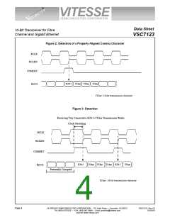
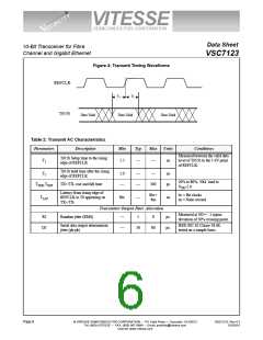
Figure 4: Transmit Timing Waveforms
REFCLK
T(0:9)
T2
T1
Data Valid
Data Valid
Data Valid
Table 2: Transmit AC Characteristics
Parameters
Description
Min
Typ
Max Units
Conditions
Measured between the valid data
level of T(0:9) to the 1.4V point
of REFCLK.
T(0:9) Setup time to the rising
edge of REFCLK
T1
1.5
—
—
ns
T(0:9) hold time after the rising
edge of REFCLK
T2
1.0
—
—
—
ns
ps
20% to 80%, 50Ω load to
VDD-2.0.
T
SDR,TSDF
TX+/TX- rise and fall time
—
300
Latency from rising edge of
REFCLK to T0 appearing on
TX+/TX-
8bc+
4ns
bc = Bit clocks
ns = Nano second
TLAT
8bc
—
ns
Transmitter Output Jitter Allocation
Measured at SO+/-, 1 sigma
deviation of 50% crossing point.
RJ
DJ
Random jitter (RMS)
—
—
5
8
ps.
ps.
Serial data output deterministic
jitter (pk-pk)
IEEE 802.3Z Clause 38.68,
tested on a sample basis.
30
80
© VITESSE SEMICONDUCTOR CORPORATION • 741 Calle Plano • Camarillo, CA 93012
Tel: (800) VITESSE • FAX: (805) 987-5896 • Email: prodinfo@vitesse.com
Internet: www.vitesse.com
Page 6
G52212-0, Rev 4.3
03/25/01

 VITESSE [ VITESSE SEMICONDUCTOR CORPORATION ]