VITESSE
SEMICONDUCTOR CORPORATION
Data Sheet
10-Bit Transceiver for Fibre
Channel and Gigabit Ethernet
VSC7123
Functional Description
Clock Synthesizer
The VSC7123 clock synthesizer multiplies the reference frequency provided on the REFCLK pin by 10 to
achieve a baud rate clock between 0.98GHz and 1.36GHz. The on-chip Phase Lock Loop (PLL) uses a single
external 0.1µF capacitor to control the Loop Filter.
Serializer
The VSC7123 accepts TTL input data as a parallel 10-bit character on the T(0:9) bus, which is latched into
the input register on the rising edge of REFCLK. This data is serialized and transmitted on the TX PECL
differential outputs at a baud rate that is 10 times the frequency of the REFCLK, with bit T0 transmitted first.
User data should be encoded using 8B/10B block code or equivalent.
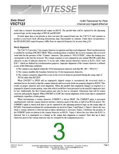
Transmission Character Interface
An encoded byte is 10 bits and is referred to as a transmission character. The 10 bit interface on the
VSC7123 corresponds to a transmission character. This mapping is illustrated in Figure 1.
Figure 1: Transmission Order and Mapping of an 8B/10B Character
Parallel Data Bits
8B/10B Bit Position
Comma Character
T9 T8 T7 T6 T5 T4 T3 T2 T1 T0
j
h
g
f
i
e
d
1
c
b
0
a
X
X
X
1
1
1
1
0
First Data Bit Transmitted
Last Data Bit Transmitted
Clock Recovery
The VSC7123 accepts differential high-speed serial inputs on the RX+/RX- pins, extracts the clock and
retimes the data. Equalizers are included in the receiver to open the data eye and compensate for InterSymbol
Interference which may be present in the incoming data. The serial bit stream should be encoded to provide DC
balance and limited run length by an 8B/10B encoding scheme. The Clock Recovery Unit is completely
monolithic and requires no external components. For proper operation, the baud rate of the data stream to be
recovered should be within +200 ppm of 10 times the REFCLK frequency. For example, Gigabit Ethernet
systems would use 125MHz oscillators with a +100ppm accuracy resulting in +200 ppm between VSC7123
pairs.
Deserializer
The recovered serial bit stream is converted into a 10-bit parallel output character. The VSC7123 provides
th
complementary TTL recovered clocks, RCLK and RCLKN, which are 1/20 of the serial baud rate. The clocks
are generated by dividing down the high-speed recovered clock, which is phase-locked to the serial data. The
© VITESSE SEMICONDUCTOR CORPORATION • 741 Calle Plano • Camarillo, CA 93012
Tel: (800) VITESSE • FAX: (805) 987-5896 • Email: prodinfo@vitesse.com
Internet: www.vitesse.com
Page 2
G52212-0, Rev 4.3
03/25/01

 VITESSE [ VITESSE SEMICONDUCTOR CORPORATION ]