VSC6134
Datasheet
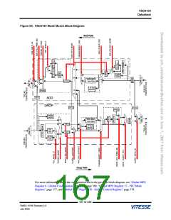
The line-side and client-side SerDes loopback clock and data are controlled separately as shown in
global register 0x014. For more information about register 0x014, see “Global MPU Register 20 -
SerDes Control Register,” page 379. The control bits are: CLIENT_DATA_LB, CLIENT_CLOCK_LB,
LINE_DATA_LB, and LINE_CLOCK_LB. If a clock loopback is not set, the transmit clock comes
from TXCLKSRCx pin. If clock loopback is set, the transmit clock comes from the looped-back
RXCLKx pin.
2.15.17 Protection Switching Mode
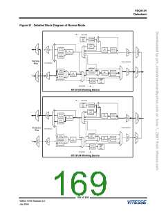
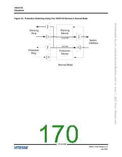
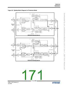
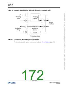
Two VSC6134 devices can be used for protection switching applications as shown in Figure 51,
page 169 and Figure 53, page 171. The data flow during the Normal mode is shown in Figure 51,
page 169 and Figure 52, page 170. The data flow after the protection switching (STS-192/STM-64 to
FEC add and drop is assumed) is shown in Figure 53, page 171 and Figure 54, page 172. In both cases,
the data flows through the VSC6134 protection device in the add path, which feeds the two high-speed
16:1 muxes. In the drop path, data flows through the working device in the normal mode. However, after
protection switching, data flows through the protection device but is looped back to the working device
such that the working device always outputs the data in the drop path.
Client side loopback for protection switching can be achieved by setting bits CLIENT_DATA_LB and
CLIENT_CLOCK_LB. For more information, see “Global MPU Register 20 - SerDes Control
Register,” page 379.
168 of 438
VMDS-10185 Revision 4.0
July 2006

 VITESSE [ VITESSE SEMICONDUCTOR CORPORATION ]