VSC6134
Datasheet
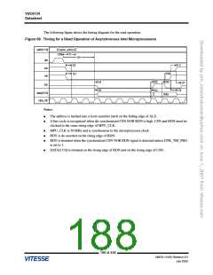
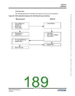
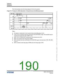
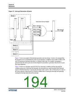
The following figure shows the timing diagram for the write operation.
Figure 70. Timing for a Write Operation of Asynchronous Intel Microprocessor
register_address
addr[11:0]
S0
H0
S5
ale
csn
wrn
H2
S2
S3
H3
D0
D5
D4
D1
rdy
Data
S4 H4
data[15:0]
mpu_clk
Notes:
●
●
The address is latched into a level-sensitive latch on the falling edge of ALE.
A bus cycle is recognized when the synchronized CSN NOR WRN is high. CSN and RDN must be
clocked to the same rising edge of MPU_CLK.
●
●
●
MPU_CLK is 50 MHz and is synchronous to the microprocessor clock.
RDY is de-asserted on the rising edge of WRN.
RDY is tristated when the synchronized CSN NOR WRN signal is detected unless DTK_TRI_PRG
is set to 1.
●
RDY is tristated on the rising edge of WRN and on the rising edge of CSN.
190 of 438
VMDS-10185 Revision 4.0
July 2006

 VITESSE [ VITESSE SEMICONDUCTOR CORPORATION ]