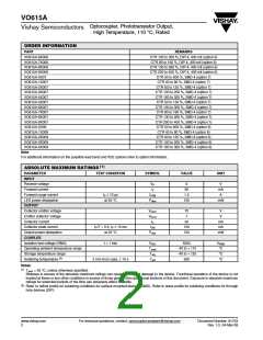
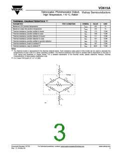
VO615A
Optocoupler, Phototransistor Output,
High Temperature, 110 °C, Rated
Vishay Semiconductors
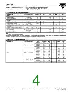
SWITCHING CHARACTERISTICS
PARAMETER
TEST CONDITION
SYMBOL
MIN
TYP.
MAX
UNIT
V
V
V
V
V
V
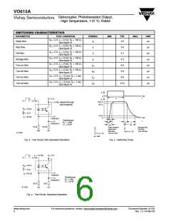
S = 5 V, IC = 2 mA, RL = 100 Ω,
Delay time
td
3.0
µs
(see figure 3)
S = 5 V, IC = 2 mA, RL = 100 Ω,
Rise time
tr
3.0
4.7
0.3
6.0
5.0
9.0
10.0
µs
µs
µs
µs
µs
µs
µs
(see figure 3)
S = 5 V, IC = 2 mA, RL = 100 Ω,
Fall time
tf
(see figure 3)
S = 5 V, IC = 2 mA, RL = 100 Ω,
Storage time
Turn-on time
Turn-off time
Turn-on time
Turn-off time
ts
(see figure 3)
S = 5 V, IC = 2 mA, RL = 100 Ω,
ton
toff
ton
toff
(see figure 3)
S = 5 V, IC = 2 mA, RL = 100 Ω,
(see figure 3)
V
V
S = 5 V, IF = 10 mA, RL = 1 kΩ,
(see figure 4)
S = 5 V, IF = 10 mA, RL = 1 kΩ,
(see figure 4)
IF
0
IC
tp
t
+ 5 V
IF
IF
0
100 %
90 %
IC = 2 mA; adjusted through
input amplitude
RG = 50
tp
= 0.01
T
10 %
tp = 50 µs
0
Channel I
tr
Oscilloscope
t
td
tf
toff
R
L = 1 M
ts
Channel II
CL = 20 pF
ton
50
100
t
t
t
t
Pulse duration
Delay time
Rise time
t
t
t
Storage time
Fall time
Turn-off time
p
d
r
on
s
f
off
(= t + t )
s
f
95 10804
(= t + t )
Turn-on time
r
d
96 11698
Fig. 3 - Test Circuit, Non-Saturated Operation
Fig. 5 - Switching Times
+ 5 V
IF
IF = 10 mA
0
IC
RG = 50 Ω
tp
= 0.01
T
tp = 50 µs
Channel I
Channel II
Oscilloscope
RL 1 MΩ
≥
≤
CL
20 pF
50 Ω
1 kΩ
95 10843
Fig. 4 - Test Circuit, Saturated Operation
www.vishay.com
6
For technical questions, contact: optocoupler.answers@vishay.com
Document Number: 81753
Rev. 1.0, 04-Mar-08

 VISHAY [ VISHAY ]