VO615A
Optocoupler, Phototransistor Output,
High Temperature, 110 °C, Rated
Vishay Semiconductors
ORDER INFORMATION
PART
REMARKS
VO615A-6X006
VO615A-7X006
VO615A-8X006
VO615A-9X006
VO615A-X007
VO615A-1X007
VO615A-2X007
VO615A-3X007
VO615A-4X007
VO615A-5X007
VO615A-6X007
VO615A-7X007
VO615A-8X007
VO615A-9X007
VO615A-X009
VO615A-1X009
VO615A-2X009
VO615A-3X009
VO615A-4X009
Note
CTR 100 to 300 %, DIP-4, 400 mil (option 6)
CTR 80 to 160 %, DIP-4, 400 mil (option 6)
CTR 130 to 260 %, DIP-4, 400 mil (option 6)
CTR 200 to 400 %, DIP-4, 400 mil (option 6)
CTR 50 to 600 %, SMD-4 (option 7)
CTR 40 to 80 %, SMD-4 (option 7)
CTR 63 to 125 %, SMD-4 (option 7)
CTR 100 to 200 %, SMD-4 (option 7)
CTR 160 to 320 %, SMD-4 (option 7)
CTR 50 to 150 %, SMD-4 (option 7)
CTR 100 to 300 %, SMD-4 (option 7)
CTR 80 to 160 %, SMD-4 (option 7)
CTR 130 to 260 %, SMD-4 (option 7)
CTR 200 to 400 %, SMD-4 (option 7)
CTR 50 to 600 %, SMD-4 (option 9)
CTR 40 to 80 %, SMD-4 (option 9)
CTR 63 to 125 %, SMD-4 (option 9)
CTR 100 to 200 %, SMD-4 (option 9)
CTR 160 to 320 %, SMD-4 (option 9)
For additional information on the possible lead bend and VDE options refer to option information.
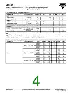
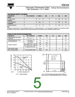
ABSOLUTE MAXIMUM RATINGS (1)
PARAMETER
TEST CONDITION
SYMBOL
VALUE
UNIT
INPUT
Reverse voltage
VR
IF
6
V
mA
A
Forward current
60
Forward surge current
LED power dissipation
OUTPUT
tP ≤ 10 µs
IFSM
Pdiss
1.5
100
at 25 °C
mW
Collector emitter voltage
Emitter collector voltage
Collector current
VCEO
VECO
IC
70
7
V
V
50
mA
mA
mW
Collector peak current
Output power dissipation
COUPLER
tP/T = 0.5, tP ≤ 10 ms
ICM
100
150
at 25 °C
Pdiss
Isolation test voltage (RMS)
Operating ambient temperature range
Storage temperature range
Soldering temperature (2)
t = 1 min
VISO
Tamb
Tstg
5000
- 40 to + 110
- 40 to + 125
260
VRMS
°C
°C
2 mm from case, ≤ 10 s
Tsld
°C
Notes
(1)
Tamb = 25 °C, unless otherwise specified.
Stresses in excess of the absolute maximum ratings can cause permanent damage to the device. Functional operation of the device is not
implied at these or any other conditions in excess of those given in the operational sections of this document. Exposure to absolute maximum
ratings for extended periods of the time can adversely affect reliability.
Refer to reflow profile for soldering conditions for surface mounted devices (SMD). Refer to wave profile for soldering conditions for through
hole devices (DIP).
(2)
www.vishay.com
2
For technical questions, contact: optocoupler.answers@vishay.com
Document Number: 81753
Rev. 1.0, 04-Mar-08

 VISHAY [ VISHAY ]