VO615A
Optocoupler, Phototransistor Output,
High Temperature, 110 °C, Rated
Vishay Semiconductors
MAXIMUM SAFETY RATINGS
PARAMETER
TEST CONDITION
SYMBOL
MIN.
TYP.
MAX.
130
UNIT
mA
INPUT
Forward current
OUTPUT
IF
Power dissipation
COUPLER
Pdiss
Tsi
265
mW
°C
Safety temperature
150
Note
According to DIN EN 60747-5-2 (VDE 0884)/DIN EN 60747-5-5 pending (see figure 1). This optocoupler is suitable for safe electrical isolation
only within the safety ratings. Compliance with the safety ratings shall be ensured by means of suitable protective circuits.
INSULATION RATED PARAMETERS
PARAMETER
TEST CONDITION
SYMBOL
MIN.
TYP.
MAX.
UNIT
Partial discharge test voltage -
routine test
100 %, ttest = 1 s
Vpd
1.6
kV
Partial discharge test voltage -
lot test (sample test)
t
Tr = 60 s, ttest = 10 s,
(see figure 2)
Vpd
1.3
kV
VIO = 500 V
RIO
RIO
1012
1011
Ω
Ω
V
V
IO = 500 V, Tamb = 100 °C
Insulation resistance
IO = 500 V, Tamb = 150 °C
(construction test only)
RIO
109
Ω
Rated impulse voltage
Max. working voltages
VIOTM
VIORM
8
kV
Recurring peak voltage
850
Vpeak
VIOTM
300
t1, t2 = 1 to 10 s
t3, t4 = 1 s
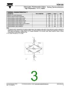
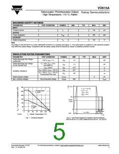
Phototransistor
Psi (mW)
250
200
150
100
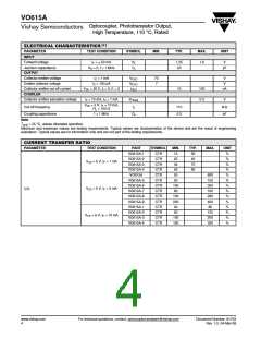
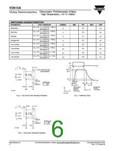
ttest = 10 s
tstres = 12 s
VPd
VIOWM
VIORM
IR-Diode
Isi (mA)
50
0
0
t3 ttest t4
t2 tstres
t
150
0
25
50
75
100 125
t1
tTr = 60 s
13930
94 9182
Tsi - Safety Temperature (°C)
Fig. 1 - Derating Diagram
Fig. 2 - Test Pulse Diagram for Sample Test According to
DIN EN 60747-5-2 (VDE 0884)/DIN EN 60747-; IEC 60747
Document Number: 81753
Rev. 1.0, 04-Mar-08
For technical questions, contact: optocoupler.answers@vishay.com
www.vishay.com
5

 VISHAY [ VISHAY ]