IRF840, SiHF840
Vishay Siliconix
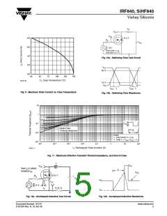
RD
VDS
VGS
8.0
6.0
4.0
2.0
0.0
D.U.T.
RG
+
V
-
DD
10 V
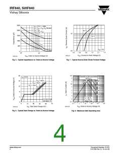
Pulse width ≤ 1 µs
Duty factor ≤ 0.1 %
Fig. 10a - Switching Time Test Circuit
VDS
90 %
25
50
75
100
125
150
TC, Case Temperature (°C)
91070_09
10 %
VGS
td(on) tr
td(off) tf
Fig. 9 - Maximum Drain Current vs. Case Temperature
Fig. 10b - Switching Time Waveforms
10
1
0 - 0.5
0.2
0.1
0.05
0.02
0.01
0.1
10-2
10-3
PDM
Single Pulse
(Thermal Response)
t1
t2
Notes:
1. Duty Factor, D = t1/t2
2. Peak Tj = PDM x ZthJC + TC
10-5
10-4
10-3
10-2
0.1
1
10
102
t1, Rectangular Pulse Duration (S)
91070_11
Fig. 11 - Maximum Effective Transient Thermal Impedance, Junction-to-Case
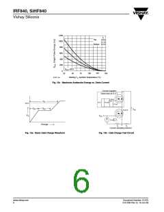
L
VDS
VDS
Vary tp to obtain
required IAS
tp
VDD
D.U.T.
+
RG
VDD
-
VDS
IAS
10 V
0.01 Ω
tp
IAS
Fig. 12a - Unclamped Inductive Test Circuit
Fig. 12b - Unclamped Inductive Waveforms
Document Number: 91070
S-81290-Rev. B, 16-Jun-08
www.vishay.com
5

 VISHAY [ VISHAY ]