10-FZ06NBA050SA-P915L33
datasheet
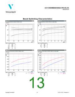
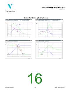
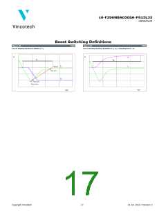
Boost Switching Characteristics
figure 15.
IGBT
figure 16.
IGBT
Typical switching times as a function of collector current
Typical switching times as a function of IGBT turn on gate resistor
t = f(IC)
t = f(Rg)
0
10
0
10
td(off)
td(on)
td(off)
td(on)
tf
tf
-1
10
-1
10
tr
tr
-2
10
-2
10
-3
10
-3
10
0
20
40
60
80
100
IC(A)
0
5
10
15
20
25
30
35
Rg(Ω)
With an inductive load at
With an inductive load at
Tj =
Tj =
150
300
±15
8
°C
V
150
300
±15
50
°C
VCE
=
=
=
=
VCE
=
=
=
V
V
A
VGE
Rgon
Rgoff
VGE
IC
V
Ω
Ω
8
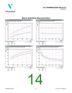
figure 17.
FWD
figure 18.
FWD
Typical reverse recovery time as a function of collector current
Typical reverse recovery time as a function of IGBT turn on gate resistor
trr = f(IC)
trr = f(Rgon)
0,30
0,25
0,20
0,15
0,10
0,05
0,00
0,45
0,40
0,35
0,30
0,25
0,20
0,15
0,10
0,05
0,00
trr
trr
trr
trr
0
20
40
60
80
100
IC(A)
0
5
10
15
20
25
30
35
R
gon(Ω)
With an inductive load at
With an inductive load at
25 °C
25 °C
Tj:
Tj:
VCE
VGE
Rgon
=
=
=
VCE
VGE
IC
=
=
=
300
±15
8
V
V
Ω
150 °C
300
±15
50
V
V
A
150 °C
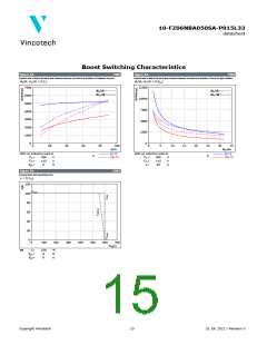
Copyright Vincotech
13
31 Jul. 2022 / Revision 3

 VINCOTECH [ VINCOTECH ]