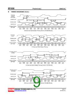
M1008
Preliminary
CMOS IC
ABSOLUTE MAXIMUM RATING
PARAMETER
SYMBOL
VDD
RATINGS
VSS-0.3 to VSS+5.5
VSS-0.3 to VDD+0.3
-25 ~ +75
UNIT
V
V
°C
°C
Supply Voltage
Input Voltage
VIN
TOPR
TSTG
Ambient Operation Temperature
Storage Temperature
-50 ~ +125
Note: Absolute maximum ratings are those values beyond which the device could be permanently damaged.
Absolute maximum ratings are stress ratings only and functional device operation is not implied.
ELECTRICAL CHARACTERISTICS (AVDD=5V, DVDD=3V, TA=25°C. Unless otherwise specified)
PARAMETER
SYMBOL
VADD
VDRDD
tMAX3
tMAX2
tMAX1
TEST CONDITION
MIN
4.75
3
30
30
TYP
5
5
MAX UNIT
Analog Power Supply
Digital Power Supply
3-Channel Mode with CDS
2-Channel Mode with CDS
1-Channel Mode with CDS
ADC Resolution
Integral Nonlinear (INL)
Differential Nonlinear (DNL)
Offset Error
5.25
5.25
V
V
MSPS
MSPS
MSPS
Bits
LSB
LSB
mV
25
16
±32
-1
-100
1
100
%FSR
VP-P
V
Gain Error
Full-Scale Input Range
Input Limits
5
2.0
5
10
1
5.85
6
-250
250
9
RFS
VI(LIMIT)
IIN
AVSS-0.3
AVDD+0.3
Input Current
nA
PGA Gain at Minimum
PGA Gain at Maximum
PGA Gain Resolution
Programmable Offset at Minimum
Programmable Offset at Maximum
Offset Resolution
V/V
V/V
Bits
mV
mV
Bits
°C
Operating
TA
0
70
Total Power Consumption
High Level Input Voltage
(CDSCLK1, CDSCLK2, ADCCLK,
Ptot
400
mW
0.8*VDD
VIH
VIL
V
V
, SCK, SLOAD)
OE
Low Level Input Voltage
(CDSCLK1, CDSCLK2, ADCCLK,
0.2*VDD
0.2*VDD
, SCK, SLOAD)
OE
0.8*VDD
High Level Input Voltage (SDATA)
Low Level Input Voltage (SDATA)
High Level Input Current
Low Level Input Current
Input Capacitance
VIH1
VIL1
IIH
IIL
CIN
V
V
uA
uA
pF
10
10
10
High Level Output Voltage
(SDATA, D0~D7)
Low Level Output Voltage
(SDATA, D0~D7)
VDD-0.5
VOH
VOL
V
V
0.5
High Level Output Current
Low Level Output Current
IOH
IOL
1
1
mA
mA
UNISONIC TECHNOLOGIES CO., LTD
4 of 11
QW-R502-434.a
www.unisonic.com.tw

 UTC [ Unisonic Technologies ]