M1008
Preliminary
CMOS IC
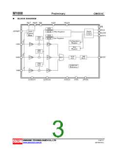
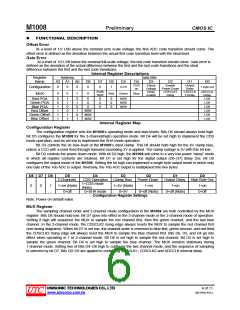
FUNCTIONAL DESCRIPTION (Cont.)
D8
D7
D6
D5
D4
D3
D2
D1
D0
Enable
Delay
1=on
CDS1
Delay
CDS2
Delay
ADCK
Delay
MUX order
Channel Select
0
1=R-G-B
(Note)
0=B-G-R
1=Red
(Note)
0=off
1=Green
0=off
(Note)
1=Blue
0=off
(Note)
1=4ns
1=4ns
1=2ns
(Note)
0=2ns
(Note)
0=2ns
(Note)
0=0ns
(Note)
0=off
MUX Register Settings
Note: Power-on default value
PGA Gain Registers
There are three PGA registers for use in respectively programming the gain of the red, green and blue
channels. Bits D8, D7 and D6 in each register must hold low, and bits D5 through D0 control the gain range in 64
increments. The coding for the PGA registers is a straight binary. An all zero word corresponds to the minimum gain
setting (1x) and an all one word corresponds to the maximum gain setting (5.85x).
The M1008 distributes one Programmable Gain Amplifier (PGA) for each channel. Each PGA has a gain range
from 1x (0dB) to 5.85x (15.3dB), adjustable in 64 steps. Although the gain curve is approximately linear in dB, the
gain in V/V varies in nonlinear proportion with the register code, according to the following the equation:
5.85
Gain =
63- G
1+ 4.85*(
)
63
Where G is the decimal value of the gain register contents, and varies from 0 to 63.
D8
0
0
0
.
D7
0
0
0
.
D6
0
0
0
.
D5
MSB
0
0
.
D4
D3
D2
D1
D0
LSB
0 (Note)
Gain(V/V) Gain(dB)
1.0
0.0
0
0
.
0
0
.
0
0
.
0
0
.
1.013
0.12
1
.
.
.
.
.
.
.
.
.
.
.
.
.
.
.
.
.
.
.
.
.
.
.
.
.
5.43
5.85
14.7
15.3
0
0
0
0
0
0
1
1
1
1
1
1
1
1
1
1
0
1
Note: Power-on default value
Offset Registers
There are three PGA registers for use in respectively programming the offset of the red, green, and blue
channels. Bits D8 through D0 control the offset range from -250mV to 250mV in 512 increments.
The coding for the offset registers is sign magnitude, with D8 as the sign bit. The following table shows the
offset range as a function of the bits D8 through D0.
D8
D7
D6
D5
D4
D3
D2
D1
D0
Offset(mV)
MSB
LSB
0
0.98
.
0
0
.
0
0
.
0
0
.
0
0
.
0
0
.
0
0
.
0
0
.
0
0
.
0 (Note)
1
.
.
.
.
.
.
.
.
.
.
.
.
.
.
.
.
.
.
.
.
.
250
0
-0.98
.
0
1
1
.
1
0
0
.
1
0
0
.
1
0
0
.
1
0
0
.
1
0
0
.
1
0
0
.
1
0
0
.
1
0
1
.
.
.
.
.
.
.
.
.
.
.
.
.
.
.
.
.
.
.
.
.
-250
1
1
1
1
1
1
1
1
1
Note: Power-on default value
UNISONIC TECHNOLOGIES CO., LTD
7 of 11
QW-R502-434.a
www.unisonic.com.tw

 UTC [ Unisonic Technologies ]