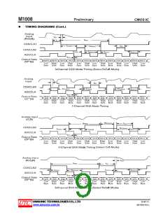
M1008
Preliminary
CMOS IC
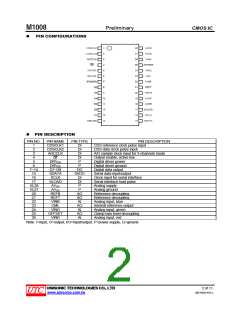
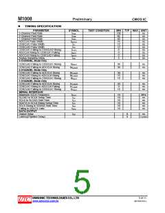
PIN CONFIGURATIONS
PIN DESCRIPTION
PIN NO.
1
PIN NAME
CDSCLK1
CDSCLK2
ADCCLK
OE
DRVDD
DRVSS
D7~D0
SDATA
SCLK
SLOAD
AVDD
AVSS
REFB
REFT
PIN TYPE
PIN DESCRIPTION
DI
DI
DI
DI
P
CDS reference clock pulse input
CDS data clock pulse input
A/D sample clock input for 3-channels mode
Output enable, active low
Digital driver power
2
3
4
5
6
P
Digital driver ground
Digital data output
7~14
15
16
DO
DI/DO
DI
DI
P
Serial data input/output
Clock input for serial interface
Serial interface load pulse
Analog supply
17
18,28
19,27
20
21
22
P
Analog ground
AO
AO
AI
Reference decoupling
Reference decoupling
Analog input, blue
VINB
23
24
CML
VING
AO
AI
Internal reference output
Analog input, green
25
26
OFFSET
VINR
AO
AI
Clamp bias level decoupling
Analog input, red
Note: I=input, O=output, I/O=input/output, P=power supply, G=ground
UNISONIC TECHNOLOGIES CO., LTD
2 of 11
QW-R502-434.a
www.unisonic.com.tw

 UTC [ Unisonic Technologies ]