uP0114
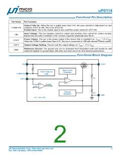
Functional Pin Description
Pin Name
Pin Function
Output Fully On. When this pin is pulled lower than 0.4V, the pass element is fully turned on and
connects VOUT to VIN. This is for uP0114A.
FON#/ EN
Enable Input. This is the enable input to turn on/off the power switch for uP0114B.
Input Voltage. This pin supplies current to output and provides bias current for control circuitry.
Bypass this pin with a minimum 2.2uF ceramic capacitor physically near the IC.
VIN
Power Output. This pin is the power output of the device that is regulated as: VOUT = 1.6 x VSET
When the FON# is pulled lower than 0.4V, this pin is connected to VIN with internal 250mΩ switch.
.
VOUT
VSET
GND
Output Voltage Setting. This pin sets the output voltage as: VOUT = 1.6 x VSET.
Reference Ground. The ground pins act as dominant heat dissipation path and should be well
soldered together to ground plane with wide and short traces for best thermal performance.
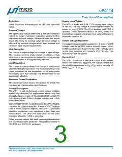
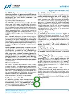
Functional Block Diagram
VIN
VOUT
Short Circuit
Protection
VOUT Fully On
Logic
FON#/ EN
R1
R2
VSET
Enable
0.8V
Thermal
Shutdown
GND
R1 = 0.6 x R2
uPI Semiconductor Corp., http://www.upi-semi.com
Rev. P00, File Name: uP0114-DS-P0000
2

 UNITPOWER [ ShenZhen XinDeYi Electronics Co., Ltd. ]