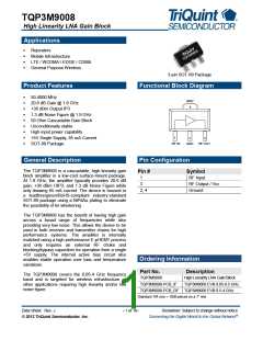
TQP3M9008
High Linearity LNA Gain Block
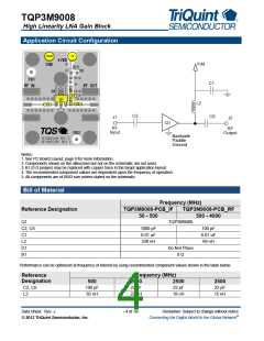
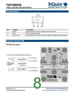
Application Circuit Configuration
J3
GND
Vdd
C1
C6
C1
Q1
L2
C6
C2
C2
J1
J2
Q1
RF
Input
RF
Output
Backside
Paddle
Ground
Notes:
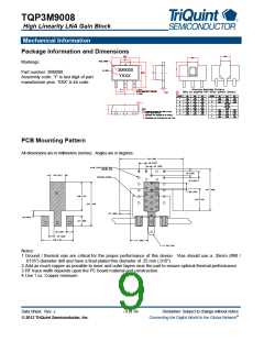
1. See PC Board Layout, page 8 for more information.
2. Components shown on the silkscreen but not on the schematic are not used.
3. B1 (0 Ω jumper) may be replaced with copper trace in the target application layout.
4. The recommended component values are dependent upon the frequency of operation.
5. All components are of 0603 size unless stated on the schematic.
Bill of Material
Frequency (MHz)
Reference Designation
TQP3M9008-PCB_IF
50 - 500
TQP3M9008-PCB_RF
500 - 4000
Q1
TQP3M9008
C2, C6
C1
1000 pF
0.01 uF
330 nH
100 pF
0.01 uF
68 nH
L2
D1
Do Not Place
0 Ω
B1
Performance can be optimized at frequency of interest by using recommended component values shown in the table below.
Frequency (MHz)
Reference
Designation
C2, C6
500
100 pF
82 nH
2000
2500
22 pF
18 nH
3500
22 pF
15 nH
22 pF
L2
22 nH
Data Sheet: Rev. J
- 4 of 10-
Disclaimer: Subject to change without notice
Connecting the Digital World to the Global Network®
© 2012 TriQuint Semiconductor, Inc.

 TRIQUINT [ TRIQUINT SEMICONDUCTOR ]