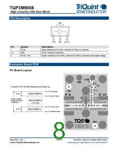
TQP3M9008
High Linearity LNA Gain Block
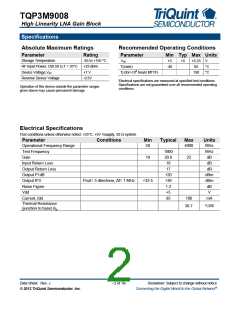
Specifications
Absolute Maximum Ratings
Recommended Operating Conditions
Parameter
Rating
-65 to +150 °C
+23 dBm
+7 V
Parameter
Vdd
Min Typ Max Units
Storage Temperature
RF Input Power, CW,50 Ω,T = 25°C
Device Voltage,Vdd
+3
+5
+5.25
V
T(case)
Tj (for>106 hours MTTF)
-40
85
°C
°C
190
Reverse Device Voltage
-0.3V
Electrical specifications are measured at specified test conditions.
Specifications are not guaranteed over all recommended operating
conditions.
Operation of this device outside the parameter ranges
given above may cause permanent damage.
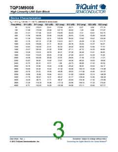
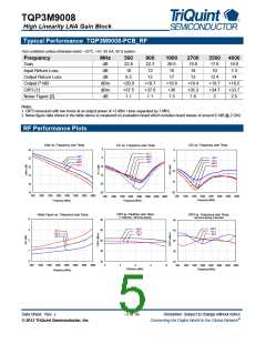
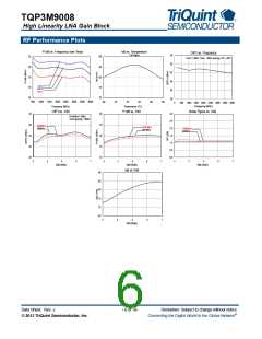
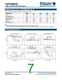
Electrical Specifications
Test conditions unless otherwise noted: +25°C, +5V Vsupply, 50 Ω system.
Parameter
Operational Frequency Range
Test Frequency
Gain
Conditions
Min
50
Typical
Max
4000
Units
MHz
MHz
dB
1900
20.6
16
19
22
Input Return Loss
Output Return Loss
Output P1dB
Output IP3
dB
17
dB
+20
+36
1.3
+5
dBm
dBm
dB
Pout= 3 dbm/tone, Δf= 1 MHz
+32.5
Noise Figure
Vdd
V
Current, Idd
85
100
mA
Thermal Resistance
(junction to base) θjb
38.7
°C/W
Data Sheet: Rev. J
- 2 of 10-
Disclaimer: Subject to change without notice
Connecting the Digital World to the Global Network®
© 2012 TriQuint Semiconductor, Inc.

 TRIQUINT [ TRIQUINT SEMICONDUCTOR ]