TMC8462 Datasheet • Document Revision V1.4 • 2018-May -09
156 / 204
7.9 SII EEPROM MFC IO Register Configuration
All MFC registers are accessible via the MFC IO Control SPI Interface. Alternatively they can be mapped into
the ESC’s Process Data RAM to allow access via EtherCAT. In this case the mapped registers can only be
written by the EtherCAT master. But they can still be read via MFC IO Control SPI Interface.
The transfer of all enabled registers is performed in one access. To enable the data update at certain
times only, a shadow register is used for every MFC register. The exact point in time when the actual data
transfer occurs (from the shadow register into a write register or from a read register into the shadow
register) is based on the chosen trigger source.
There is one configuration byte in the SII EEPROM (and ESC Parameter RAM respectively) for each MFC
block register. The configuration for all registers has the same options:
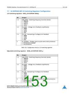
Bit
3:0
4
Description
Trigger Source
Enable RAM transfer
0 : disabled, register access only from MCU via MFC CTRL SPI
1 : enabled, read and write access via EtherCAT, readable by MCU via MFC CTRL SPI
7:5
Unused
Table 196: Register configuration byte
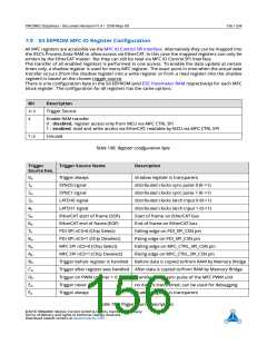
Trigger
Source hex.
Trigger Source Name
Description
0h
1h
2h
3h
4h
5h
6h
7h
8h
9h
Ah
Bh
Ch
Dh
Eh
Fh
Trigger always
shadow register is transparent
SYNC0 signal
distributed clocks sync pulse 0 (0->1)
distributed clocks sync pulse 1 (0->1)
distributed clocks latch input 0 (0->1)
distributed clocks latch input 1 (0->1)
Start of frame on EtherCAT bus
SYNC1 signal
LATCH0 signal
LATCH1 signal
EtherCAT start of frame (SOF)
EtherCAT end of frame (EOF)
PDI SPI nCS=0 (Chip Select)
PDI SPI nCS=1 (Chip Deselect)
MFC SPI nCS=0 (Chip Select)
MFC SPI nCS=1 (Chip Deselect)
End of frame on EtherCAT bus
Falling edge on PDI_SPI_CSN pin
Rising edge on PDI_SPI_CSN pin
Falling edge on MFC_CTRL_SPI_CSN pin
Rising edge on MFC_CTRL_SPI_CSN pin
Trigger before register is handled Before data is copied to/from RAM by Memory Bridge
Trigger after register was handled After data is copied to/from RAM by Memory Bridge
Trigger on PWM counter = 0
Trigger never
Transfer at the zero pulse of the MFC PWM unit
no data is transferred, can be used for debugging
shadow register is transparent
Trigger always
Table 197: Trigger source descriptions
©2018 TRINAMIC Motion Control GmbH & Co. KG, Hamburg, Germany
Terms of delivery and rights to technical change reserved.
Download newest version at www.trinamic.com

 TRINAMIC [ TRINAMIC MOTION CONTROL GMBH & CO. KG. ]