TMC8462 Datasheet • Document Revision V1.4 • 2018-May -09
155 / 204
7.8 SII EEPROM MFC IO Memory Block Mapping
The MFC registers can be mapped to specific memory areas to allow EtherCAT access, so that the data is
directly copied between each register and the assigned memory location. This allows the operation with a
less powerful application processor or even without an application processor at all in Device Emulation
mode.
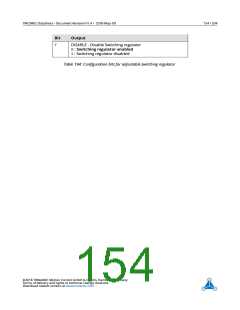
The registers are dynamically mapped to one of two memory blocks:
• Memory Block 0 is used for write-registers (data direction: EtherCAT master -> MFC register)
• Memory Block 1 is used for read-registers (data direction: MFC register -> EtherCAT master).
The start address of each memory block can be configured to be anywhere in the process data RAM (1000h
to (4FFFh-blocksize)).
The length of each block depends on the selected registers that are mapped into the block. Extra care
should be taken that the blocks do not overlap each other, that they do not overlap with other process
data in the DPRAM, and that the memory blocks’ start addresses are not too close at 4FFFh.
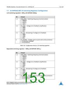
Memory Block 0 base address 059Fh:059Eh (SII EEPROM: 00A3h:00A2h)
The start address of the block that all write registers of the MFC are mapped into.
Address 059Fh contains the upper byte of the start address. Allowed values: 10h...4Fh
Address 059Eh contains the lower byte of the start address. Allowed values: 00h...FFh
Memory Block 1 base address 05A1h:05A0h (SII EEPROM: 00A5h:00A4h)
The start address of the block that all read registers of the MFC are mapped into.
Address 059Fh contains the upper byte of the start address. Allowed values: 10h...4Fh
Address 059Eh contains the lower byte of the start address. Allowed values: 00h...FFh
When a register is mapped to the RAM for EtherCAT transfer, its memory address depends on the other
enabled registers with a lower register number.
The start address of any enabled register will be a multiple of 4 bytes from the start address of the memory
block. Between registers that are not a multiple of 4 bytes, a padding gap is left that is not transferred.
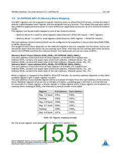
For example if a 2 byte register, a 8 byte register a 1 byte register and a 4 byte register are enabled in a
memory block starting at 2000h, the memory is used as shown in this table:
Register
Reg. 1 (2 byte) 2001h
Padding 2003h
End Address Start Address
2000h
2002h
2004h
200Ch
200Dh
2010h
Reg. 2 (8 byte) 200Bh
Reg. 3 (1 byte) 200Ch
Padding
200Fh
Reg. 4 (4 byte) 2013h
Table 195: Register mapping example
For the actual register sizes please refer to Table 124 in Section 7.2.
©2018 TRINAMIC Motion Control GmbH & Co. KG, Hamburg, Germany
Terms of delivery and rights to technical change reserved.
Download newest version at www.trinamic.com

 TRINAMIC [ TRINAMIC MOTION CONTROL GMBH & CO. KG. ]