TMC6200 DATASHEET (Rev. 1.01 / 2018-NOV-15)
33
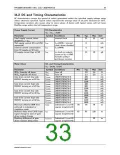
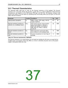
11.2 DC and Timing Characteristics
DC characteristics contain the spread of values guaranteed within the specified supply voltage range
unless otherwise specified. Typical values represent the average value of all parts measured at +25°C.
Temperature variation also causes stray to some values. A device with typical values will not leave
Min/Max range within the full temperature range.
Power Supply Current
DC-Characteristics
VVS = VVSA = 24.0V
Parameter
Symbol Conditions
Min
Typ
Max Unit
Total supply current, driver
disabled IVS + IVSA
IS
internal clock
11
15
mA
VSA supply current (VS and VSA IVSA
separated)
fCLK=24MHz / internal
clock, driver disabled
fCLK=24MHz
8
6
mA
mA
µA
Internal current consumption
from 5V supply on VCC pin
IO supply current (typ. at 5V)
IVCC
IVIO
no load on outputs,
inputs at VIO or GND
Excludes pullup /
15
30
pull-down resistors
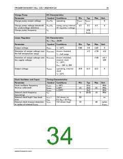
Motor Driver
Parameter
DC- and Timing-Characteristics
VVS = 24.0V; Tj=50°C
Symbol Conditions
Min
Typ
Max Unit
RDSON lowside off driver
RDSON highside off driver
Gate drive current low side
MOSFET turning on at 2V VGS
RONL
RONH
Gate off
Gate off
1.0
1.3
400
800
1200
400
800
1200
600
1200
1800
600
1200
1800
50
1.6
2.0
Ω
Ω
ISLPON0
ISLPON2
ISLPON3
ISLPON0
ISLPON2
ISLPON3
ISLPOFF0
ISLPOFF2
ISLPOFF3
ISLPOFF0
ISLPOFF2
ISLPOFFN3
tBBM0
DRIVESTRENGTH=0
DRIVESTRENGTH=2
DRIVESTRENGTH=3
DRIVESTRENGTH=0
DRIVESTRENGTH=2
DRIVESTRENGTH=3
DRIVESTRENGTH=0
DRIVESTRENGTH=2
DRIVESTRENGTH=3
DRIVESTRENGTH=0
DRIVESTRENGTH=2
DRIVESTRENGTH=3
Individual LS and HS
signals (singleline=0)
mA
mA
mA
mA
mA
mA
mA
mA
mA
mA
mA
mA
ns
Gate drive current high side
MOSFET turning on at 2V VGS
Gate drive current low side
MOSFET turning off at 4V VGS
Gate drive current high side
MOSFET turning on at 4V VGS
Minimum effective BBM time
enforced in individual or
singleline mode
Reaction delay time LS/HS input tDLY
signal change to start of gate
driver output change
30
65
70
110
10
Individual LS and HS
signals (singleline=0)
85
ns
ns
Matching difference of gate
driver reaction delay times
tDLYMATCH
Individual LS and HS
signals (singleline=0)
www.trinamic.com

 TRINAMIC [ TRINAMIC MOTION CONTROL GMBH & CO. KG. ]