TMC5160 DATASHEET (Rev. 1.08 / 2018-NOV-19)
120
28.2 DC and Timing Characteristics
DC characteristics contain the spread of values guaranteed within the specified supply voltage range
unless otherwise specified. Typical values represent the average value of all parts measured at +25°C.
Temperature variation also causes stray to some values. A device with typical values will not leave
Min/Max range within the full temperature range.
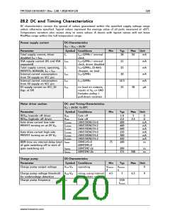
Power supply current
DC-Characteristics
VVS = VVSA = 24.0V
Parameter
Total supply current, driver
disabled IVS + IVSA
Symbol Conditions
Min
Typ
18
Max Unit
24 mA
IS
fCLK=12MHz / internal
clock
VSA supply current (VS and VSA IVSA
separated)
fCLK=12MHz / internal
clock, driver disabled
fCLK=12MHz, 23.4kHz
chopper, no load
fCLK=12MHz
15
25
mA
mA
mA
mA
µA
Total supply current, operating,
MOSFETs AOD4126, IVS + IVSA
Internal current consumption
from 5V supply on VCC pin
Internal current consumption
from 5V supply on VCC pin
IO supply current on VCC_IO
(typ. at 5V)
IS
IVCC
IVCC
IVIO
10
fCLK=16MHz
12.5
15
no load on outputs,
inputs at VIO or GND
Excludes pullup /
30
pull-down resistors
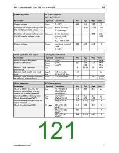
Motor driver section
Parameter
DC- and Timing-Characteristics
VVS = 24.0V; Tj=50°C
Symbol Conditions
Min
Typ
Max Unit
RDSON lowside off driver
RDSON highside off driver
Gate drive current low side
MOSFET turning on at 2V VGS
RONL
RONH
Gate off
Gate off
1.8
2.2
3
3.5
Ω
Ω
ISLPON0
ISLPON2
ISLPON3
ISLPON0
ISLPON2
ISLPON3
DRVSTRENGTH=0
DRVSTRENGTH=2
DRVSTRENGTH=3
DRVSTRENGTH=0
DRVSTRENGTH=2
DRVSTRENGTH=3
BBMCLKS=0
200
400
600
150
300
450
100
mA
mA
mA
mA
mA
mA
ns
Gate drive current high side
MOSFET turning on at 2V VGS
BBM time via internal delay (start tBBM0
of gate switching off to start of
75
BBMTIME=0
gate switching on)
tBBM16
tBBM16
BBMTIME=16
BBMTIME=24
200
375
ns
ns
500
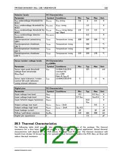
Charge pump
DC-Characteristics
Parameter
Symbol Conditions
Min
Typ
Max Unit
Charge pump output voltage
VVCP-VVS
VVCP-VVS
fCP
operating
V12VOUT - V12VOUT
-
V
2
1
Charge pump voltage threshold
for undervoltage detection
Charge pump frequency
rising, using internal
5V regulator voltage
4.5
5
6.5
V
1/16
fCLKOSC
www.trinamic.com

 TRINAMIC [ TRINAMIC MOTION CONTROL GMBH & CO. KG. ]