TMC5160 DATASHEET (Rev. 1.08 / 2018-NOV-19)
121
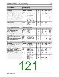
Linear regulator
DC-Characteristics
VVS = VVSA = 24.0V
Parameter
Symbol Conditions
Min
Typ
5.0
Max Unit
Output voltage
V5VOUT
TJ = 25°C
4.80
5.20
V
Deviation of output voltage over V5VOUT(DEV) drivers disabled
the full temperature range
+/-30
+/-100
mV
TJ = full range
Deviation of output voltage over V5VOUT(DEV) drivers disabled,
+/-50
12.2
mV /
10V
the full supply voltage range
internal clock
TA = 25°C
VVSA = 10V to 30V
Output voltage
V12VOUT
operating, internal
clock
10.8
11.5
V
TJ = 25°C
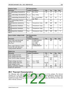
Clock oscillator and input
Parameter
Clock oscillator frequency
(factory calibrated)
Timing-Characteristics
Symbol Conditions
Min
Typ
11.7
12.0
12.1
10-16
Max Unit
MHz
fCLKOSC
fCLKOSC
fCLKOSC
fCLK
tJ=-50°C
tJ=50°C
tJ=150°C
11.5
4
12.5
MHz
MHz
MHz
External clock frequency
(operating)
18
External clock high / low level
time
External clock timeout detection tCLKH1
in cycles of internal fCLKOSC
tCLKH
tCLKL
/
CLK driven to
0.1 VVIO / 0.9 VVIO
CLK driven high
10
32
ns
48
cycles
fCLKOSC
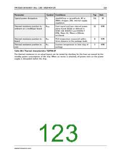
Short detection
Parameter
DC-Characteristics
Symbol Conditions
Min
Typ
Max Unit
Short to GND / Short to VS
detector delay (Start of gate
switch on to short detected)
Including 100ns filtering time
Short detector level S2VS
(measurement includes drop in
sense resistor)
tSD0
FILT_ISENSE=0
S2xx_LEVEL=6
shortdelay=0
shortdelay=1
S2VS_LEVEL=15
S2VS_LEVEL=6
0.5
0.85
1.1
µs
tSD1
VBM
1.1
1.4
0.55
1.6
1.56
0.625
2.2
1.72
0.70
µs
V
V
Short detector level S2G
VS - VBM
S2G_LEVEL=15;
VS<52V
S2G_LEVEL=15;
VS<55V
S2G_LEVEL=6;
VS<50V
1.2
1.56
1.9
V
V
V
0.85
0.46
0.625
0.80
www.trinamic.com

 TRINAMIC [ TRINAMIC MOTION CONTROL GMBH & CO. KG. ]