TMC5160 DATASHEET (Rev. 1.08 / 2018-NOV-19)
124
29 Layout Considerations
29.1 Exposed Die Pad
The TMC5160 uses its die attach pad to dissipate heat from the gate drivers and the linear regulator to
the board. For best electrical and thermal performance, use a reasonable amount of solid, thermally
conducting vias between the die attach pad and the ground plane. The printed circuit board should
have a solid ground plane spreading heat into the board and providing for a stable GND reference.
29.2 Wiring GND
All signals of the TMC5160 are referenced to their respective GND. Directly connect all GND pins under
the device to a common ground area (GND, GNDP, GNDA and die attach pad). The GND plane right
below the die attach pad should be treated as a virtual star point. For thermal reasons, the PCB top
layer shall be connected to a large PCB GND plane spreading heat within the PCB.
Attention
Place the TMC5160 near to the MOSFET bridge and sense resistor GND in order to avoid ringing
leading to GND differences and to dangerous inductive peak voltages.
29.3 Wiring Bridge Supply
The power bridge will draw the full coil current in pulses with extremely high dI/dt. Thus, any
inductivity between VS supply filtering and the MOSFETs can lead to severe voltage spikes. This has to
be avoided. Avoid any bend in the supply traces between filtering capacitors and MOSFET switches,
and keep distance as small as possible. Especially for high current, use a separate plane for the supply
voltage, and a sufficient number and capacity for supply filtering. Use an additional capacitor for the
IC VS pin, as additional ripple voltage would cause severe current spikes on the charge pump
capacitor. A tiny series resistor can be added to avoid this.
Attention
Keep supply voltage ripple low, by using sufficient filtering capacity close to the MOSFET bridge.
29.4 Supply Filtering
The 5VOUT output voltage ceramic filtering capacitor (2.2 to 4.7 µF recommended) should be placed as
close as possible to the 5VOUT pin, with its GND return going directly to the GNDA pin. This ground
connection shall not be shared with other loads or additional vias to the GND plane. Use as short and
as thick connections as possible. For best microstepping performance and lowest chopper noise an
additional filtering capacitor should be used for the VCC pin to GND, to avoid digital part ripple
influencing motor current regulation. Therefore, place a ceramic filtering capacitor (470nF
recommended) as close as possible (1-2mm distance) to the VCC pin with GND return going to the
ground plane. VCC can be coupled to 5VOUT using a 2.2 Ω or 3.3 Ω resistor in order to supply the
digital logic from 5VOUT while keeping ripple away from this pin. A 100 nF filtering capacitor should
be placed as close as possible to the VSA pin to ground plane. Make sure, that VS does not see
excessive voltage spikes caused by bridge operation and place a 100 nF or larger filter capacitor to
GND close to the VS pin.
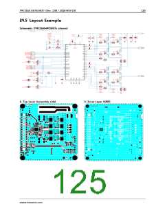
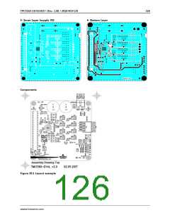
Please carefully read chapters 3.3 and 3.4 to understand the special considerations with regard to
layout and component selection for the external MOSFET power bridges.
www.trinamic.com

 TRINAMIC [ TRINAMIC MOTION CONTROL GMBH & CO. KG. ]